Module 2 - Introduction to AVR Assembly
1. Introduction to AVR Assembly Language
Assembly is a low-level programming language that allows manipulation of every bit in memory, resulting in highly efficient and fast code. It has a strong one-to-one correspondence with the machine code instructions of the computer architecture.
On Arduino microcontrollers (specifically the ATmega328P), Assembly programming enables high-level control suitable for real-time systems and applications requiring complex mathematical processes.
Advantages of Using Assembly:
- High efficiency: Full control over memory usage and execution time.
- Deep understanding: Helps understand fundamental microcontroller operations.
- Problem solving: Can solve problems that may arise in other high-level languages.
Disadvantages:
- Steep learning curve: Requires deep understanding of hardware architecture.
- Longer code: For simple tasks, Assembly code is much longer compared to high-level languages.
2. ATmega328P Hardware & Memory Architecture
A. Memory Map
The ATmega328P memory map provides information on how the Microcontroller Unit (MCU) uses memory. Here is the address division:
| Category |
Address |
Size |
Description |
| General Purpose Registers |
0x0000 - 0x001F |
32 x 8 bit |
Registers R0 - R31 |
| I/O Registers |
0x0020 - 0x005F |
64 x 8 bit |
Accessible via IN/OUT instructions |
| Extended I/O Registers |
0x0060 - 0x00FF |
160 x 8 bit |
Additional I/O registers |
| Internal SRAM |
0x0100 - 0x08FF |
2048 x 8 bit |
Internal data memory |
B. General Purpose Working Registers (GPR)
The AVR architecture has 32 general-purpose registers labeled R0 through R31. These registers function as temporary storage for data during processing and are directly connected to the ALU (Arithmetic Logic Unit).
Register Division:
| Group |
Registers |
Characteristics |
| Lower Registers |
R0 - R15 |
Limited functionality. Cannot store immediate values directly (cannot use LDI instruction). |
| Upper Registers |
R16 - R31 |
More flexible. Can work with immediate data, allowing direct storage of bytes or words. |
Pointer Registers:
The last six registers (R26 through R31) can be combined into 16-bit pointers for indirect memory addressing:
| Pointer Name |
Low Register |
High Register |
Function |
| X Register |
R26 (XL) |
R27 (XH) |
Pointer for memory access |
| Y Register |
R28 (YL) |
R29 (YH) |
Pointer for memory access |
| Z Register |
R30 (ZL) |
R31 (ZH) |
Pointer for memory & flash access |
3. Input/Output (I/O) Programming
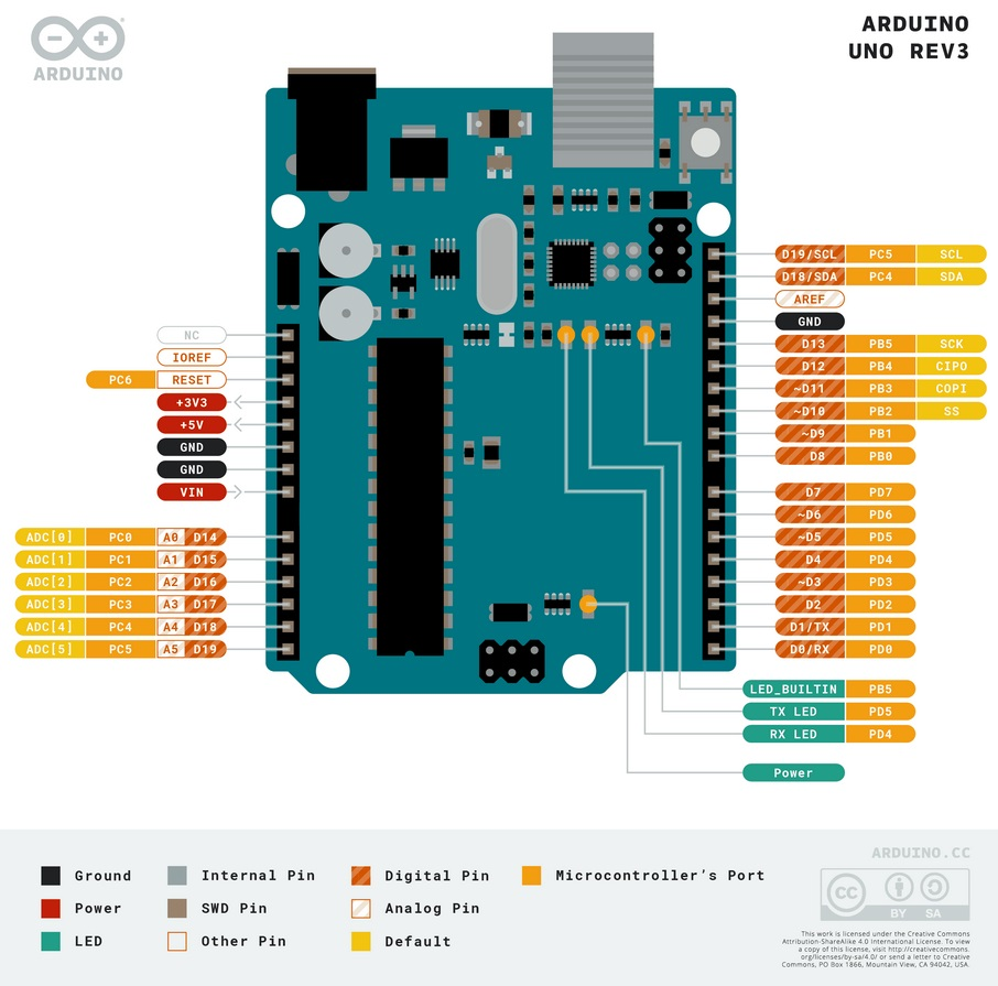
On the Arduino Uno (ATmega328P), digital I/O is controlled through Port B, Port C, and Port D. Each port is 8-bit, allowing control of up to 8 pins simultaneously.

A. Port to Arduino Pin Mapping
| Port |
Bits |
Arduino Pin |
Notes |
| Port B |
PB0 - PB5 |
Digital Pin 8 - 13 |
PB6-PB7 are used for crystal oscillator |
| Port C |
PC0 - PC5 |
Analog Pin A0 - A5 |
PC6 is the RESET pin |
| Port D |
PD0 - PD7 |
Digital Pin 0 - 7 |
PD0 (RX) and PD1 (TX) for serial communication |
B. Main I/O Registers
Three main registers control the behavior of each port:
| Register |
Full Name |
Access |
Function |
| DDRx |
Data Direction Register |
Read/Write |
Configures pin direction. 0 = Input, 1 = Output |
| PORTx |
Data Register |
Read/Write |
If Output: Sets logic High (1) or Low (0). If Input: Activates internal Pull-up resistor (1) or Tri-state (0) |
| PINx |
Input Pins Address |
Read Only |
Reads the physical logic state of the pin (0 or 1) |
(Replace 'x' with Port name, e.g., DDRB, PORTB, PINB)
C. Register Bit Configuration Details
DDRx - Data Direction Register
| DDRx Bit Value |
Pin Direction |
Explanation |
| 0 |
Input |
Pin is configured as input (high impedance) |
| 1 |
Output |
Pin is configured as output (source/sink current) |
PORTx - Data Register (Depends on DDRx Configuration)
| DDRx |
PORTx |
Mode |
Pin Condition |
| 0 (Input) |
0 |
Tri-state (Hi-Z) |
Pin is floating, no pull-up |
| 0 (Input) |
1 |
Input Pull-up |
Internal pull-up resistor active, pin defaults to HIGH |
| 1 (Output) |
0 |
Output Low |
Pin outputs 0V (GND) |
| 1 (Output) |
1 |
Output High |
Pin outputs 5V (VCC) |
| PINx Bit Value |
Pin Status |
Explanation |
| 0 |
LOW |
Pin voltage is below threshold (near 0V) |
| 1 |
HIGH |
Pin voltage is above threshold (near 5V) |
4. Assembly Integration with Arduino IDE
To combine Assembly with Arduino C++ code, the extern "C" directive is used in the .ino file and the .global directive is used in the .S (Assembly) file.
File Structure:
.ino File (C/C++):
extern "C" {
  void start();    // Declaration of function defined in Assembly
  void loop_asm(); // Another function from Assembly
}

void setup() {
  start();         // Call Assembly function for initialization
}

void loop() {
  loop_asm();      // Call Assembly function for main loop
}
.S File (Assembly):
#define __SFR_OFFSET 0x00
#include "avr/io.h"

.global start
.global loop_asm

start:
    SBI DDRB, 5      ; Set PB5 (Pin 13) as Output
    RET              ; Return to caller

loop_asm:
    SBI PORTB, 5     ; Turn on LED
    ; ... other code
    RET
Directive Explanations:
#define __SFR_OFFSET 0x00: Sets the offset for I/O registers to use symbolic names (DDRB, PORTB, etc.).#include "avr/io.h": Includes register definitions for the AVR chip..global: Makes label/function accessible from other files (exported symbol).RET: Instruction to return from subroutine to the calling program.
5. AVR Assembly Instruction Set
Operand Notation
Before diving into the instructions, here are the common operand symbols used:
| Symbol |
Description |
| Rd |
Destination register (R0-R31). The result of the operation is stored here. |
| Rr |
Source register (R0-R31). Used as input for the operation. |
| K |
Constant/Immediate value (8-bit: 0-255 or 0x00-0xFF). |
| k |
Address constant for SRAM or program memory. |
| A |
I/O register address (0-63 for IN/OUT, 0-31 for SBI/CBI). |
| b |
Bit number (0-7) within a register or I/O address. |
| X, Y, Z |
Pointer registers (X=R27:R26, Y=R29:R28, Z=R31:R30). |
Note: Some instructions only work with upper registers (R16-R31), such as LDI, ANDI, ORI, SUBI, SBCI, and CPI.
A. Data Transfer Instructions
Used to move data between registers or between registers and memory/I/O.
| Mnemonic |
Operand |
Description |
Example |
Notes |
| LDI |
Rd, K |
Load Immediate |
LDI R16, 0xFF |
Loads 8-bit constant K into register Rd (R16-R31 only) |
| MOV |
Rd, Rr |
Move/Copy Register |
MOV R0, R1 |
Copies contents of register Rr to Rd |
| IN |
Rd, A |
Input from I/O |
IN R16, PINB |
Reads data from I/O port A to register Rd |
| OUT |
A, Rr |
Output to I/O |
OUT PORTB, R16 |
Sends data from register Rr to I/O port A |
| LDS |
Rd, k |
Load from SRAM |
LDS R16, 0x0100 |
Loads data from SRAM address k to register Rd |
| STS |
k, Rr |
Store to SRAM |
STS 0x0100, R16 |
Stores register Rr contents to SRAM address k |
| LD |
Rd, X/Y/Z |
Load Indirect |
LD R16, X |
Loads data from address pointed by pointer X/Y/Z |
| ST |
X/Y/Z, Rr |
Store Indirect |
ST X, R16 |
Stores data to address pointed by pointer X/Y/Z |
| PUSH |
Rr |
Push to Stack |
PUSH R16 |
Saves register to stack |
| POP |
Rd |
Pop from Stack |
POP R16 |
Retrieves data from stack to register |
B. Bit Manipulation Instructions (I/O Specific)
These instructions operate on the lower 32 I/O addresses ($00-$1F). Very efficient for changing one bit without affecting other bits.
| Mnemonic |
Operand |
Description |
Example |
Notes |
| SBI |
A, b |
Set Bit in I/O |
SBI DDRB, 5 |
Sets bit b in I/O register A to 1 |
| CBI |
A, b |
Clear Bit in I/O |
CBI PORTB, 5 |
Clears bit b in I/O register A to 0 |
| BST |
Rr, b |
Bit Store to T |
BST R16, 3 |
Copies bit b from register Rr to T flag |
| BLD |
Rd, b |
Bit Load from T |
BLD R17, 5 |
Copies T flag to bit b of register Rd |
C. Arithmetic Instructions
| Mnemonic |
Operand |
Description |
Example |
Notes |
| ADD |
Rd, Rr |
Add |
ADD R1, R2 |
Rd = Rd + Rr |
| ADC |
Rd, Rr |
Add with Carry |
ADC R1, R2 |
Rd = Rd + Rr + C (Carry flag) |
| SUB |
Rd, Rr |
Subtract |
SUB R16, R17 |
Rd = Rd - Rr |
| SBC |
Rd, Rr |
Subtract with Carry |
SBC R16, R17 |
Rd = Rd - Rr - C |
| SUBI |
Rd, K |
Subtract Immediate |
SUBI R16, 10 |
Rd = Rd - K (R16-R31 only) |
| SBCI |
Rd, K |
Subtract Immediate with Carry |
SBCI R17, 0 |
Rd = Rd - K - C |
| INC |
Rd |
Increment |
INC R16 |
Rd = Rd + 1 |
| DEC |
Rd |
Decrement |
DEC R16 |
Rd = Rd - 1 |
| MUL |
Rd, Rr |
Multiply Unsigned |
MUL R16, R17 |
R1:R0 = Rd × Rr (16-bit result) |
| MULS |
Rd, Rr |
Multiply Signed |
MULS R16, R17 |
R1:R0 = Rd × Rr (signed) |
| NEG |
Rd |
Negate (Two's Complement) |
NEG R16 |
Rd = 0x00 - Rd |
D. Logic Instructions
| Mnemonic |
Operand |
Description |
Example |
Notes |
| AND |
Rd, Rr |
Logical AND |
AND R1, R2 |
Rd = Rd AND Rr |
| ANDI |
Rd, K |
AND Immediate |
ANDI R16, 0x0F |
Rd = Rd AND K (masking) |
| OR |
Rd, Rr |
Logical OR |
OR R1, R2 |
Rd = Rd OR Rr |
| ORI |
Rd, K |
OR Immediate |
ORI R16, 0x80 |
Rd = Rd OR K |
| EOR |
Rd, Rr |
Exclusive OR |
EOR R16, R17 |
Rd = Rd XOR Rr |
| COM |
Rd |
One's Complement |
COM R16 |
Rd = 0xFF - Rd (inverts all bits) |
| CLR |
Rd |
Clear Register |
CLR R16 |
Rd = 0 (same as EOR Rd, Rd) |
| SER |
Rd |
Set Register |
SER R16 |
Rd = 0xFF (R16-R31 only) |
E. Shift & Rotate Instructions
| Mnemonic |
Operand |
Description |
Example |
Notes |
| LSL |
Rd |
Logical Shift Left |
LSL R16 |
Shift left, bit 0 = 0, bit 7 → Carry |
| LSR |
Rd |
Logical Shift Right |
LSR R16 |
Shift right, bit 7 = 0, bit 0 → Carry |
| ROL |
Rd |
Rotate Left through Carry |
ROL R16 |
Rotate left through Carry flag |
| ROR |
Rd |
Rotate Right through Carry |
ROR R16 |
Rotate right through Carry flag |
| ASR |
Rd |
Arithmetic Shift Right |
ASR R16 |
Shift right, bit 7 remains (preserve sign) |
| SWAP |
Rd |
Swap Nibbles |
SWAP R16 |
Swaps upper and lower 4-bits in register |
F. Branch & Control Flow Instructions
| Mnemonic |
Operand |
Description |
Example |
Notes |
| RJMP |
k |
Relative Jump |
RJMP loop |
Jump to label k (±2K words) |
| JMP |
k |
Jump |
JMP far_label |
Jump to 22-bit address (all memory) |
| RCALL |
k |
Relative Call |
RCALL delay |
Call subroutine relative to PC |
| CALL |
k |
Call |
CALL far_sub |
Call subroutine at 22-bit address |
| RET |
- |
Return |
RET |
Return from subroutine |
| RETI |
- |
Return from Interrupt |
RETI |
Return from interrupt handler |
| CP |
Rd, Rr |
Compare |
CP R16, R17 |
Compare Rd with Rr (updates flags) |
| CPI |
Rd, K |
Compare Immediate |
CPI R16, 5 |
Compare Rd with constant K |
| CPC |
Rd, Rr |
Compare with Carry |
CPC R17, R19 |
For multi-byte comparison |
| BREQ |
k |
Branch if Equal |
BREQ target |
Jump if Z flag = 1 (result equal) |
| BRNE |
k |
Branch if Not Equal |
BRNE loop |
Jump if Z flag = 0 (result not equal) |
| BRLO |
k |
Branch if Lower |
BRLO less |
Jump if C flag = 1 (unsigned <) |
| BRSH |
k |
Branch if Same or Higher |
BRSH greater |
Jump if C flag = 0 (unsigned ≥) |
| BRLT |
k |
Branch if Less Than |
BRLT neg |
Jump if S flag = 1 (signed <) |
| BRGE |
k |
Branch if Greater or Equal |
BRGE pos |
Jump if S flag = 0 (signed ≥) |
G. Skip Instructions
| Mnemonic |
Operand |
Description |
Example |
Notes |
| SBIS |
A, b |
Skip if Bit in I/O Set |
SBIS PINB, 0 |
Skip next instruction if bit = 1 |
| SBIC |
A, b |
Skip if Bit in I/O Cleared |
SBIC PIND, 2 |
Skip next instruction if bit = 0 |
| SBRS |
Rr, b |
Skip if Bit in Register Set |
SBRS R16, 7 |
Skip if bit b in register = 1 |
| SBRC |
Rr, b |
Skip if Bit in Register Cleared |
SBRC R16, 0 |
Skip if bit b in register = 0 |
H. Other Instructions
| Mnemonic |
Operand |
Description |
Example |
Notes |
| NOP |
- |
No Operation |
NOP |
Does nothing (1 clock cycle) |
| SLEEP |
- |
Sleep |
SLEEP |
Enters sleep mode (power saving) |
| WDR |
- |
Watchdog Reset |
WDR |
Resets watchdog timer |
| SBIW |
Rd, K |
Subtract Immediate from Word |
SBIW R24, 1 |
Subtract K from 16-bit value (R25:R24) |
| ADIW |
Rd, K |
Add Immediate to Word |
ADIW R24, 1 |
Add K to 16-bit value |
6. Status Register (SREG)
The Status Register contains flags that indicate the results of arithmetic/logic operations. This register is crucial for branch instructions.
| Bit |
Name |
Description |
| 7 |
I (Global Interrupt Enable) |
Enables/disables global interrupts |
| 6 |
T (Bit Copy Storage) |
Storage for BLD/BST instructions |
| 5 |
H (Half Carry Flag) |
Carry from bit 3 to bit 4 (for BCD) |
| 4 |
S (Sign Flag) |
S = N ⊕ V (for signed operations) |
| 3 |
V (Overflow Flag) |
Two's complement overflow |
| 2 |
N (Negative Flag) |
Result is negative (bit 7 = 1) |
| 1 |
Z (Zero Flag) |
Result = 0 |
| 0 |
C (Carry Flag) |
Carry/borrow from operation |
7. Delay Implementation Without Library
Delays can be created using nested loops that consume a certain number of clock cycles.
Delay Calculation Concept:
- ATmega328P on Arduino Uno runs at 16 MHz (16 million clock cycles per second)
- 1 millisecond = 16,000 clock cycles
DEC instruction takes 1 cycle, BRNE takes 2 cycles (if branch taken)
Delay Implementation Examples:
; Delay approximately 1 second (with nested loop)
delay_1s:
    LDI R18, 64          ; Outer counter
outer_loop:
    LDI R24, lo8(62500)  ; Inner counter low byte
    LDI R25, hi8(62500)  ; Inner counter high byte
inner_loop:
    SBIW R24, 1          ; Subtract 16-bit counter (2 cycles)
    BRNE inner_loop      ; Loop if not 0 (2 cycles if taken)
    DEC R18              ; Subtract outer counter
    BRNE outer_loop      ; Loop outer if not 0
    RET

; Simple delay with single loop
delay_simple:
    LDI R16, 255         ; Load counter
delay_loop:
    DEC R16              ; Decrement counter (1 cycle)
    BRNE delay_loop      ; Branch if not zero (2 cycles)
    RET                  ; Return (approximately 765 cycles total)
8. Complete Program Examples
A. Blink LED
#define __SFR_OFFSET 0x00
#include "avr/io.h"

.global main

main:
    SBI DDRB, 5          ; Set PB5 (Pin 13) as Output

loop:
    SBI PORTB, 5         ; Turn on LED (Output HIGH)
    RCALL delay          ; Call delay subroutine
    CBI PORTB, 5         ; Turn off LED (Output LOW)
    RCALL delay          ; Call delay subroutine
    RJMP loop            ; Repeat continuously

delay:
    LDI R18, 82          ; Outer loop counter
outer:
    LDI R24, lo8(60000)  ; Inner loop counter (low byte)
    LDI R25, hi8(60000)  ; Inner loop counter (high byte)
inner:
    SBIW R24, 1          ; Subtract word (R25:R24)
    BRNE inner           ; Loop if not 0
    DEC R18              ; Subtract outer counter
    BRNE outer           ; Loop outer if not 0
    RET                  ; Return to caller
#define __SFR_OFFSET 0x00
#include "avr/io.h"

.global main

main:
    ; Setup
    SBI DDRB, 5          ; PB5 (Pin 13) as Output (LED)
    CBI DDRD, 2          ; PD2 (Pin 2) as Input (Button)
    SBI PORTD, 2         ; Activate Pull-up on PD2

loop:
    SBIC PIND, 2         ; Skip next instruction if button pressed (LOW)
    RJMP led_off         ; If not pressed, turn off LED

led_on:
    SBI PORTB, 5         ; Turn on LED
    RJMP loop            ; Return to loop

led_off:
    CBI PORTB, 5         ; Turn off LED
    RJMP loop            ; Return to loop
C. Toggle LED with Button (Simple Debounce)
#define __SFR_OFFSET 0x00
#include "avr/io.h"

.global main

main:
    ; Initialization
    SBI DDRB, 5          ; PB5 as Output (LED)
    CBI DDRD, 2          ; PD2 as Input (Button)
    SBI PORTD, 2         ; Activate internal Pull-up
    CLR R20              ; R20 = LED status (0 = off)

wait_press:
    SBIC PIND, 2         ; Wait for button pressed (LOW)
    RJMP wait_press

    ; Button pressed - toggle LED
    SBRC R20, 0          ; Skip if bit 0 of R20 = 0 (LED off)
    RJMP turn_off

turn_on:
    SBI PORTB, 5         ; Turn on LED
    LDI R20, 1           ; Set status = on
    RJMP debounce

turn_off:
    CBI PORTB, 5         ; Turn off LED
    CLR R20              ; Set status = off

debounce:
    RCALL delay          ; Delay for debounce

wait_release:
    SBIS PIND, 2         ; Wait for button released (HIGH)
    RJMP wait_release
    RCALL delay          ; Delay debounce after release
    RJMP wait_press      ; Return to wait for press

delay:
    LDI R18, 50
d_outer:
    LDI R24, lo8(10000)
    LDI R25, hi8(10000)
d_inner:
    SBIW R24, 1
    BRNE d_inner
    DEC R18
    BRNE d_outer
    RET