Module 5 - Timer
- 1. Introduction to AVR Timers
- 2. Operating Modes
- 3. Timer0
- 4. Timer1
- 5. Delay Using Timers
- 6. Der Code
1. Introduction to AVR Timers
1.1. Overview
The ATmega328P is a widely popular 8-bit microcontroller, serving as the "brain" for many embedded systems, most notably the Arduino Uno. Among its most critical peripherals are the Timers. These components allow the microcontroller to perform time-sensitive tasks without stalling the CPU, such as measuring time intervals, generating PWM (Pulse Width Modulation) signals, or triggering specific events at precise moments.
The ATmega328P is equipped with three internal timers:
- Timer0: 8-bit timer (counts from 0 to 255).
- Timer1: 16-bit timer (counts from 0 to 65,535).
- Timer2: 8-bit timer (counts from 0 to 255).
Note: This module only covers Timer0 and Timer1. If you want to know more about Timer2, you can read the ATMega328p Documentation.
1.2. Technical Specifications Overview

While all three timers share similar logic, they differ in resolution and specific features.
| Timer | Resolution | Common Use Case | Pins |
|---|---|---|---|
| Timer0 | 8-bit | Basic time-slicing for multitasking, polling loops, and simple hardware PWM. | PD6 (OC0A), PD5 (OC0B) |
| Timer1 | 16-bit | High-resolution input capture (measuring pulse width), precise frequency generation, and 16-bit event counting. | PB1 (OC1A), PB2 (OC1B) |
| Timer2 | 8-bit | Asynchronous clocking (using a 32kHz crystal on TOSC1/2), real-time counters, and PWM. | PB3 (OC2A), PD3 (OC2B) |
2. Operating Modes
2.1. Normal Mode

In Normal Mode, the timer acts as a simple up-counter. It starts from 0 and increments with every clock pulse (after passing through the prescaler) until it reaches its maximum value (0xFF for 8-bit, 0xFFFF for 16-bit.
Once it hits the maximum, it "rolls over" or overflows back to 0. Upon overflow, the Timer Overflow Flag (TOVn) is set, which can trigger an Interrupt Service Routine (ISR). This is perfect for tracking elapsed time by incrementing a software counter every time an overflow occurs.
Formula for Overflow Frequency:
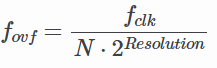
where N is the prescaler value.
2.2. CTC (Clear Timer on Compare) Mode

CTC Mode is far more precise for generating specific frequencies. Instead of waiting for an overflow at the maximum possible value, the timer counts until it matches a value you pre-defined in the Output Compare Register (OCRnx). As soon as the match occurs, the timer clears itself (resets to 0).
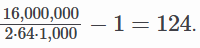
You can configure the timer to "toggle" an output pin automatically when the match occurs, creating a perfect square wave without CPU intervention. For example, to generate a 1 kHz square wave using a 16 MHz clock and a 64 prescaler, you would calculate the required OCR value:
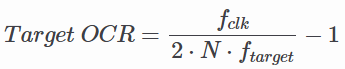
Using the values above:
2.3. PWM (Pulse Width Modulation) Mode
PWM Mode is used to simulate an analog output using digital signals. By rapidly switching a pin between HIGH and LOW, you can control the average power delivered to a component.
- Fast PWM: High frequency, suitable for power regulation and LED dimming. The timer counts from 0 to MAX, resetting to 0 immediately. The output pin changes state when the timer reaches the OCR value.
- Phase Correct PWM: Provides a symmetrical waveform by counting up to MAX and then counting back down to 0. This is preferred for motor control as it reduces electromagnetic noise. Duty Cycle: Controlled by the value in the OCR register. A higher value means the signal stays "HIGH" longer within one period.
3. Timer0
3.1. TCNT0 (Timer/Counter 0 Register)

The TCNT0 register is the core component of the 8-bit TIMER0 module. It acts as the actual counter that holds the current timer value. The value of TCNT0 increments (or decrements in certain PWM modes) based on the selected clock source and prescaler.
Users can read from or write to this register at any time. Note that manually writing a value to TCNT0 while the timer is running can cause the timer to "miss" a Compare Match with the OCR0x registers. This happens because the hardware comparison occurs in the clock cycle following a TCNT0 update.
In PWM modes, TCNT0 is constantly compared against OCR0A and OCR0B. When the values match, the output pins (OC0A/OC0B) toggle, clear, or set, depending on the configuration.
3.2. TCCR0 (Timer/Counter 0 Control Register)
In the ATmega328P, the control functionality is split into two registers: TCCR0A and TCCR0B. Together, they define the timer's behavior, including waveform generation, output modes, and clock scaling.
3.2.1. TCCR0A (Control Register A)

- Bit 7:6 - COM0A1:0 (Compare Match Output Mode A): Controls the behavior of the OC0A pin when TCNT0 matches OCR0A.
- Bit 5:4 - COM0B1:0 (Compare Match Output Mode B): Controls the behavior of the OC0B pin when TCNT0 matches OCR0B.
- Bit 1:0 - WGM01:0 (Wave Generation Mode): Combined with WGM02 in TCCR0B to select the timer mode (Normal, CTC, Fast PWM, Phase Correct PWM).
3.2.1.1. COM0x1:0 Description
This table shows the COM0x1:0 functionality when the timer is in a non-PWM mode (normal or CTC):
| COM0x1 | COM0x0 | Description |
|---|---|---|
| 0 | 0 | Normal port operation, OC0x disconnected. |
| 0 | 1 | Toggle OC0x on Compare Match. |
| 1 | 0 | Clear OC0x on Compare Match (Set output to low). |
| 1 | 1 | Set OC0x on Compare Match (Set output to high). |
3.2.1.2. WGM02:0 Description
This table shows how the WGM02:0 bits affect the counting sequence of the counter, the source for maximum (TOP) counter value, and what type of waveform generation to be used:
| WGM02 | WGM01 | WGM00 | Timer/Counter Mode of Operation | TOP | Update of OCRx at | TOV Flag Set on |
|---|---|---|---|---|---|---|
| 0 | 0 | 0 | Normal | 0xFF | Immediate | MAX |
| 0 | 0 | 1 | PWM, phase correct | 0xFF | TOP | BOTTOM |
| 0 | 1 | 0 | CTC | OCRA | Immediate | MAX |
| 0 | 1 | 1 | Fast PWM | 0xFF | BOTTOM | MAX |
| 1 | 0 | 0 | Reserved | — | — | — |
| 1 | 0 | 1 | PWM, phase correct | OCRA | TOP | BOTTOM |
| 1 | 1 | 0 | Reserved | — | — | — |
| 1 | 1 | 1 | Fast PWM | OCRA | BOTTOM | TOP |
Notes:
- MAX: 0xFF
- BOTTOM: 0x00
- Update of OCRx at: When the hardware actually updates the value of the Compare Register if you change it while the timer is running.
3.2.2. TCCR0B (Control Register B)

- Bit 7 - FOC0A (Force Output Compare A): Only active in non-PWM modes. Writing
1forces an immediate match on OC0A. - Bit 6 - FOC0B (Force Output Compare B): Only active in non-PWM modes. Writing
1forces an immediate match on OC0B. - Bit 3 - WGM02 (Waveform Generation Mode): Works with WGM01:0 to set the mode.
- Bit 2:0 - CS02:0 (Clock Select): Sets the prescaler or selects an external clock source.
3.2.2.1. CS02:0 Prescaler Settings
| CS02 | CS01 | CS00 | Description |
|---|---|---|---|
| 0 | 0 | 0 | No clock source (Timer/Counter stopped) |
| 0 | 0 | 1 | clk / 1 (No prescaling) |
| 0 | 1 | 0 | clk / 8 (From prescaler) |
| 0 | 1 | 1 | clk / 64 (From prescaler) |
| 1 | 0 | 0 | clk / 256 (From prescaler) |
| 1 | 0 | 1 | clk / 1024 (From prescaler) |
| 1 | 1 | 0 | External clock source on T0 pin. Clock on falling edge. |
| 1 | 1 | 1 | External clock source on T0 pin. Clock on rising edge. |
3.3. TIFR0 (Timer/Counter 0 Interrupt Flag Register)

- Bit 2 - OCF0B (Output Compare Flag B): Set to
1when TCNT0 matches the value in OCR0B. - Bit 1 - OCF0A (Force Output Compare A): Set to
1when TCNT0 matches the value in OCR0A. - Bit 0 - TOV0 (Timer Overflow Flag): Set to
1when the timer overflows (reaches its MAX value and restarts from 0).
4. Timer1
4.1. TCNT1 (Timer/Counter Register)

TCNT1 is functionally the same as TCNT0, serving as the core counter for its respective module, with several significant additions and architectural differences. TCNT1 is a 16-bit register divided into two 8-bit register, TCNT1H (high byte) and TCNT1L (low byte). This allows it to count from 0 to 65,535, providing much higher precision and longer timing.
TCNT1 includes a specialized Input Capture feature not found in Timer0. When a signal event occurs on the ICP1 pin, the current value of TCNT1 is instantly copied into the ICR1 register. This is used to measure external pulse widths with high accuracy.
4.2. TCCR1 (Timer/Counter 1 Control Register)
4.2.1. TCCR1A (Control Register A)

- Bit 7:6 - COM10A1:0 (Compare Match Output Mode A): Controls the behavior of the OC1A pin when TCNT1 matches OCR1A.
- Bit 5:4 - COM1B1:0 (Compare Match Output Mode B): Controls the behavior of the OC1B pin when TCNT1 matches OCR1B.
- Bit 1:0 - WGM11:0 (Wave Generation Mode): Combined with WGM13:12 in TCCR1B to select one of 16 available modes.
4.2.1.1. COM1x1:0 Description
This table shows the COM1x1:0 functionality when the timer is in a non-PWM mode (normal or CTC):
| COM1x1 | COM1x0 | Description |
|---|---|---|
| 0 | 0 | Normal port operation, OC1x disconnected. |
| 0 | 1 | Toggle OC1x on Compare Match. |
| 1 | 0 | Clear OC1x on Compare Match (Set output to low). |
| 1 | 1 | Set OC1x on Compare Match (Set output to high). |
4.2.1.2. WGM13:0 Description
This table shows how the WGM13:0 bits affect the counting sequence of the counter, the source for maximum (TOP) counter value, and what type of waveform generation to be used:
| Mode | WGM13 | WGM12 | WGM11 | WGM10 | Timer/Counter Mode of Operation | TOP | Update of OCR1x at | TOV1 Flag Set on |
|---|---|---|---|---|---|---|---|---|
| 0 | 0 | 0 | 0 | 0 | Normal | 0xFFFF | Immediate | MAX |
| 1 | 0 | 0 | 0 | 1 | PWM, phase correct, 8-bit | 0x00FF | TOP | BOTTOM |
| 2 | 0 | 0 | 1 | 0 | PWM, phase correct, 9-bit | 0x01FF | TOP | BOTTOM |
| 3 | 0 | 0 | 1 | 1 | PWM, phase correct, 10-bit | 0x03FF | TOP | BOTTOM |
| 4 | 0 | 1 | 0 | 0 | CTC | OCR1A | Immediate | MAX |
| 5 | 0 | 1 | 0 | 1 | Fast PWM, 8-bit | 0x00FF | BOTTOM | TOP |
| 6 | 0 | 1 | 1 | 0 | Fast PWM, 9-bit | 0x01FF | BOTTOM | TOP |
| 7 | 0 | 1 | 1 | 1 | Fast PWM, 10-bit | 0x03FF | BOTTOM | TOP |
| 8 | 1 | 0 | 0 | 0 | PWM, phase and frequency correct | ICR1 | BOTTOM | BOTTOM |
| 9 | 1 | 0 | 0 | 1 | PWM, phase and frequency correct | OCR1A | BOTTOM | BOTTOM |
| 10 | 1 | 0 | 1 | 0 | PWM, phase correct | ICR1 | TOP | BOTTOM |
| 11 | 1 | 0 | 1 | 1 | PWM, phase correct | OCR1A | TOP | BOTTOM |
| 12 | 1 | 1 | 0 | 0 | CTC | ICR1 | Immediate | MAX |
| 13 | 1 | 1 | 0 | 1 | (Reserved) | — | — | — |
| 14 | 1 | 1 | 1 | 0 | Fast PWM | ICR1 | BOTTOM | TOP |
| 15 | 1 | 1 | 1 | 1 | Fast PWM | OCR1A | BOTTOM | TOP |
4.2.2. TCCR1B (Control Register B)

- Bit 7 - ICNC1 (Input Capture Noise Canceler): When set to
1, a digital filter is activated on the ICP1 pin. It requires four matching cycles to trigger, reducing noise spikes. - Bit 6 - ICES1 (Input Capture Edge Select): Selects which edge triggers a capture on the ICP1 pin.
1= Rising edge;0= Falling edge. - Bit 3 - WGM13:2 (Waveform Generation Mode): Works with WGM11:0 to set the mode.
- Bit 2:0 - CS12:0 (Clock Select): Sets the prescaler or selects an external clock source.
4.2.2.1. CS02:0 Prescaler Settings
| CS12 | CS11 | CS10 | Description |
|---|---|---|---|
| 0 | 0 | 0 | No clock source (Timer/Counter stopped) |
| 0 | 0 | 1 | clk / 1 (No prescaling) |
| 0 | 1 | 0 | clk / 8 (From prescaler) |
| 0 | 1 | 1 | clk / 64 (From prescaler) |
| 1 | 0 | 0 | clk / 256 (From prescaler) |
| 1 | 0 | 1 | clk / 1024 (From prescaler) |
| 1 | 1 | 0 | External clock source on T0 pin. Clock on falling edge. |
| 1 | 1 | 1 | External clock source on T0 pin. Clock on rising edge. |
4.2.3. TCCR1C (Control Register C)

- Bit 7 - FOC1A (Force Output Compare A): Only active in non-PWM modes. Writing
1forces an immediate match on OC1A. - Bit 6 - FOC1B (Force Output Compare B): Only active in non-PWM modes. Writing
1forces an immediate match on OC1B.
4.3. TIFR1 (Timer/Counter 1 Interrupt Flag Register)

- Bit 5 - ICF1 (Input Capture Flag): Set to
1when a capture event occurs on the ICP1 pin. - Bit 2 - OCF1B (Output Compare Flag B): Set to
1when TCNT1 matches the value in OCR1B. - Bit 1 - OCF1A (Force Output Compare A): Set to
1when TCNT1 matches the value in OCR1A. - Bit 0 - TOV1 (Timer Overflow Flag): Set to
1when the timer overflows (reaches its MAX value and restarts from 0).
5. Delay Using Timers
5.1. Delay Calculation in Normal Mode
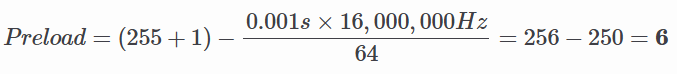
In Normal Mode, the timer always counts up to its maximum value and then overflows. To get a specific delay, you preload the TCNTn register with a starting value so it only has to count a specific number of steps before overflowing.
Here is the formula to find the required preload value:
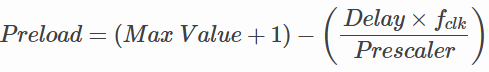
For example, if we want to create a 1ms delay using Timer0 with 1/64 presacaler:
5.2. Delay Calculation in CTC Mode
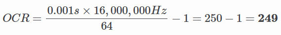
In CTC (Clear Timer on Compare) Mode, the timer is much easier to use for delays because the hardware automatically resets the counter to zero when it reaches a target value stored in the OCRnx (Output Compare Register).
Here is the formula to find the value to put in OCRnx register:
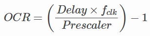
For example, if we want to create a 1ms delay using Timer0 with 1/64 presacaler:
6. Der Code
6.1. Code Example 1 (Timer0)
This code toggles PD5 every 0.5s. The delay_timer0 subroutine uses Timer0 in CTC Mode with a 1024 prescaler and a compare value of 156, creating a 10ms hardware delay per call. This subroutine is called 50 times using software loop with R18 as the counter.
;------------------------
; Assembly Code
;------------------------
#define __SFR_OFFSET 0x00
#include "avr/io.h"
;------------------------
.global main
;===============================================================
    main:
    LDI R16, 0b00100000 ; to toggle PD5
    LDI R17, 0b00000000
    ;--------------------------------------------
    SBI DDRD, 5         ; set PD5 for o/p
    OUT PORTD, R17      ; PD5 = 0
    ;--------------------------------------------
    LDI R18, 50         ; set loop counter
l1: RCALL delay_timer0  ; apply delay via timer0
    DEC R18
    BRNE l1             ; & go back & repeat
    ;--------------------------------------------
    EOR R17, R16        ; R17 = R17 XOR R16
    OUT PORTD, R17      ; toggle PD5
    LDI R18, 50         ; re-set loop counter
    RJMP l1             ; go back & repeat toggle
;===============================================================
delay_timer0:           ; ~10ms delay via Timer0
    ;---------------------------------------------------------
    CLR R20
    OUT TCNT0, R20      ; initialize timer0 with count=0
    LDI R20, 156
    OUT OCR0A, R20      ; OCR0 = 9
    LDI R20, 0b00000010
    OUT TCCR0A, R20
    LDI R20, 0b00000101
    OUT TCCR0B, R20     ; timer0: CTC mode, prescaler 1024
    ;---------------------------------------------------------
l2: IN R20, TIFR0       ; get TIFR0 byte & check
    SBRS R20, OCF0A     ; if OCF0=1, skip next instruction
    RJMP l2             ; else, loop back & check OCF0 flag
    ;---------------------------------------------------------
    CLR R20
    OUT TCCR0B, R20     ; stop timer0
    ;---------------------------------------------------------
    LDI R20, (1<<OCF0A)
    OUT TIFR0, R20      ; clear OCF0 flag
    RET
6.2. Code Example 2 (Timer1)
This code toggles PD5 every 0.5s (just like Code Example 1). The delay_timer1 subroutine uses Timer1 in Normal Mode with a 1024 prescaler and a preload value of 57724, creating a 500ms hardware delay per call.
;------------------------
; Assembly Code
;------------------------
#define __SFR_OFFSET 0x00
#include "avr/io.h"
;------------------------
.global main
;===============================================================
main:
    LDI R16, 0b00100000 ; to toggle PD5
    LDI R17, 0b00000000
    ;---------------------------------------------
    SBI DDRD, 5         ; set PD5 for o/p
    OUT PORTD, R17      ; PD5 = 0
    ;---------------------------------------------
l1: RCALL delay_timer1  ; 0.5 sec delay via timer1
    ;---------------------------------------------
    EOR R17, R16        ; R17 = R17 XOR R16
    OUT PORTD, R17      ; toggle PD5
    LDI R18, 61         ; re-set loop counter
    RJMP l1             ; go back & repeat toggle
;===============================================================
delay_timer1:           ; 0.5 sec delay via timer1
;-------------------------------------------------------
    .EQU value, 57724   ; value to give 0.5 sec delay
    LDI R20, hi8(value)
    STS TCNT1H, R20
    LDI R20, lo8(value)
    STS TCNT1L, R20     ; initialize counter TCNT1 = value
    ;-------------------------------------------------------
    LDI R20, 0b00000000
    STS TCCR1A, R20
    LDI R20, 0b00000101
    STS TCCR1B, R20     ; normal mode, prescaler = 1024
    ;-------------------------------------------------------
l2: IN R20, TIFR1       ; get TIFR1 byte & check
    SBRS R20, TOV1      ; if TOV1=1, skip next instruction
    RJMP l2             ; else, loop back & check TOV1 flag
    ;-------------------------------------------------------
    LDI R20, 1<<TOV1
    OUT TIFR1, R20      ; clear TOV1 flag
    ;-------------------------------------------------------
    LDI R20, 0b00000000
    STS TCCR1B, R20     ; stop timer1
    RET