Module 7 - PWM and EEPROM
1. PWM (Pulse Width Modulation)
PWM is a technique used to simulate analog output using a digital signal. Instead of producing a true analog voltage, the microcontroller rapidly switches a pin between HIGH and LOW.
| Term | Meaning |
|---|---|
| Period | Total time of one cycle |
| Duty Cycle | Percentage of time signal is HIGH |
Changing the duty cycle changes the average voltage seen by external devices.
AVR microcontrollers provide hardware timers that can automatically generate PWM signals in the background. It basically switches on and off on certain positions of the counter. To generate more finely controlled PWM output (such as those for servos), Timer1 is usually used as it is 16 bits thus allowing more precise features.
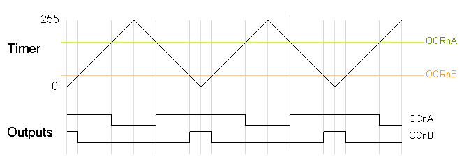
Phase Correct PWM
Phase correct PWM uses dual slop that goes up and down, switching between those operations. This mode performs more accurately in exchange for half the available frequency.
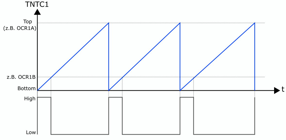
Fast PWM
Fast PWM provides PWM with higher frequency but lower resolution because it uses a single-slope operation, where the counter immediately returns to 0 after reaching its maximum value. Fast PWM is commonly used for devices that require high-frequency signals.
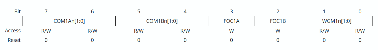
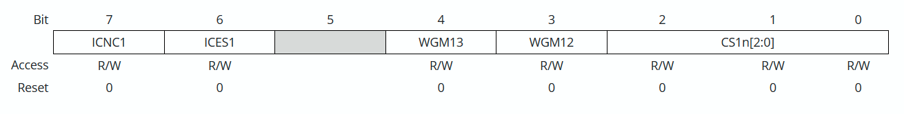
TCCRnA and TCCRnB — Timer/Counter Control Registers
TCR1A
TCR1B
COM
| COM1x1 | COM1x0 | Description |
|---|---|---|
| 0 | 0 | Normal port operation (PWM disconnected) |
| 0 | 1 | Toggle OC1X on Compare Match (special case) |
| 1 | 0 | Clear on Compare Match, Set at BOTTOM (Non-inverting PWM) |
| 1 | 1 | Set on Compare Match, Clear at BOTTOM (Inverting PWM) |
WGM
Certain modes in the Timer that affects PWM behavior
| Mode | WGM13 | WGM12 | WGM11 | WGM10 | Mode Name | TOP |
|---|---|---|---|---|---|---|
| 1 | 0 | 0 | 0 | 1 | PWM Phase Correct 8-bit | 0x00FF |
| 2 | 0 | 0 | 1 | 0 | PWM Phase Correct 9-bit | 0x01FF |
| 3 | 0 | 0 | 1 | 1 | PWM Phase Correct 10-bit | 0x03FF |
| 5 | 0 | 1 | 0 | 1 | Fast PWM 8-bit | 0x00FF |
| 6 | 0 | 1 | 1 | 0 | Fast PWM 9-bit | 0x01FF |
| 7 | 0 | 1 | 1 | 1 | Fast PWM 10-bit | 0x03FF |
| 8 | 1 | 0 | 0 | 0 | PWM Phase & Frequency Correct (ICR1) | ICR1 |
| 9 | 1 | 0 | 0 | 1 | PWM Phase & Frequency Correct (OCR1A) | OCR1A |
| 10 | 1 | 0 | 1 | 0 | PWM Phase Correct (ICR1) | ICR1 |
| 11 | 1 | 0 | 1 | 1 | PWM Phase Correct (OCR1A) | OCR1A |
| 14 | 1 | 1 | 1 | 0 | Fast PWM (ICR1 TOP) | ICR1 |
| 15 | 1 | 1 | 1 | 1 | Fast PWM (OCR1A TOP) | OCR1A |
OCRn — Output Compare Register
The Output Compare Register stores a value that the timer constantly compares against the counter. When the counter hits that value, it triggers compare match that does different things aaccording to COM to the set output pin.
- Setting a pin HIGH
- Clearing a pin LOW
- Triggering an interrupt
ICRn — Input Capture Register
The Input Capture Register is used in certain PWM modes as the TOP value of the timer. This means the timer counts from 0 up to the value stored in ICRn before restarting the counting cycle.
When used as TOP, ICRn determines the PWM period (frequency).
In PWM modes that use ICRn as TOP (such as mode 8 & 15), the timer behavior becomes:
Counter: 0 → ICRn → reset
Changing ICRn changes the PWM frequency, while OCRn still controls the duty cycle.
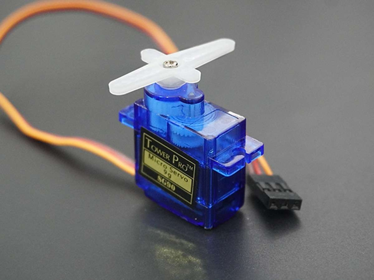
2. Servos
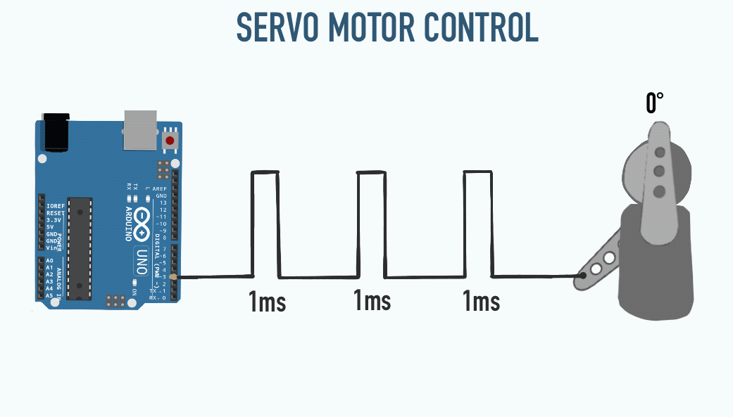
Servos are motors that adjusts to certain angles following certain PWM pulses.
Servo Signal Operation
Servo operates with 20 ms PWM periods.
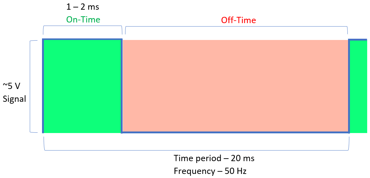
| Parameter | Typical Value |
|---|---|
| PWM Period | ≈ 20 ms |
| Pulse Width | ≈ 1 – 2 ms |
Servo operates with 20 ms PWM periods. This can hardly be achieved with Timer0 since Timer0 is an 8-bit timer.
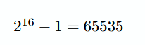
This means its maximum counter value is:
2^8 - 1 = 255
20 ms period is hardly achievable with this which requires a 16-bit timer is preferred.
This allows precise generation of long PWM periods.
Using a prescaler of 8:
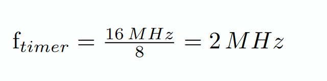
Timer tick duration:

Required servo period: 20 ms
Number of timer counts required:

Servo Initialization Code Example
SBI DDRB, 1
Configure OC1A pin as output. Timer1 will control this pin automatically.
LDI R22, (1<<COM1A1) | (1<<WGM11)
STS TCCR1A, R22
TCCR1A configuration:
| Bit | Purpose |
|---|---|
| COM1A1 = 1 | Enable PWM output on OC1A |
| WGM11 = 1 | Part of Fast PWM mode selection |
This connects Timer1 to the output pin.
LDI R22, hi8(40000)
STS ICR1H, R22
LDI R22, lo8(40000)
STS ICR1L, R22
Set ICR1 = 40000.
This is to make the Timer 1 count to 40 000 following the previous calculations.
LDI R22, (1<<WGM13) | (1<<WGM12) | (1<<CS11)
STS TCCR1B, R22
TCCR1B configuration:
| Bit | Purpose |
|---|---|
| WGM13 + WGM12 | Complete Fast PWM Mode 14 |
| CS11 = 1 | Prescaler = 8 |
This starts Timer1 in Fast PWM mode.
Servo Initialization
; Sets Timer1 PWM in PB1 to use period of 20ms by using Fast PWM.
; Timer1 counts until ICR1
SERVO_init:
  SBI DDRB, 1

  LDI R22, (1<<COM1A1) | (1<<WGM11)
  STS TCCR1A, R22

  LDI R22, hi8(40000)
  STS ICR1H, R22
  LDI R22, lo8(40000)
  STS ICR1L, R22

  LDI R22, (1<<WGM13) | (1<<WGM12) | (1<<CS11)
  STS TCCR1B, R22

  RET
Servo Usage
  .EQU LEFT, 2400  ; Generates a 2400/40000 % duty cycle.

  LDI R16, hi8(LEFT)
  STS OCR1AH, R16
  LDI R16, lo8(LEFT)
  STS OCR1AL, R16
This code makes the PWM generate compare match at count 2400 this allows it to produce a 2400/40000 * 20 ms = ~1.2 ms pulse which is around 0 degrees.
3. EEPROM
EEPROM is a small non-volatile memory inside the microcontroller.
Unlike SRAM:
- SRAM loses data when power is removed
- EEPROM keeps data even after reset or power loss
EEPROM is commonly used to store:
- Settings
- Calibration values
- System state
EEPROM has limited write endurance, so it should only be used sparingly
EEPROM Registers
EEPROM operations are controlled using dedicated I/O registers.
EEARH:EEARL — EEPROM Address Register
Stores the memory address to be accessed.
EEDR — EEPROM Data Register
Stores the data to be written or read.
EECR — EEPROM Control Register
Controls read and write operations.
Important control bits:
| Name | Bit | Function |
|---|---|---|
| EERE | 0 | EEPROM Read Enable |
| EEWE | 1 | EEPROM Write Enable |
| EEMWE | 2 | EEPROM Host Write Enable |
EEPROM Write Operation
Writing EEPROM requires a specific sequence:
- Wait until EEWE becomes ‘0’.
- Write new EEPROM address to EEAR (optional).
- Write new EEPROM data to EEDR (optional).
- Write a logical ‘1’ to the EEMWE bit while writing a ‘0’ to EEWE in EECR.
- Within four clock cycles after setting EEMWE, write a logical ‘1’ to EEWE.
; Writes R21 to EEPROM address in 0x0052
EEPROM_write:
  SBIC  EECR, 1
  RJMP  EEPROM_write

  LDI R22, hi8(0x0052)
  OUT   EEARH, R22
  LDI R22, lo8(0x0052)
  OUT   EEARL, R22

  OUT   EEDR, R21

  SBI   EECR, 2
  SBI   EECR, 1
  RET
EEPROM Read Operation
Reading EEPROM is simpler:
- Load address into EEAR
- Start read operation by setting EERE
- Read data from EEDR
; Read R21 from EEPROM address in 0x0052
EEPROM_read:
  SBIC  EECR, 1
  RJMP  EEPROM_read

  LDI R22, hi8(0x0052)
  OUT   EEARH, R22
  LDI R22, lo8(0x0052)
  OUT   EEARL, R22

  SBI   EECR, 0
  IN    R21, EEDR
  RET