Embedded System (MBD)
- Module 1 - Setup
- Module 2 - Introduction to AVR Assembly
- 1. Introduction to AVR Assembly Language
- 2. ATmega328P Hardware & Memory Architecture
- 3. Input/Output (I/O) Programming
- 4. Assembly Integration with Arduino IDE
- 5. AVR Assembly Instruction Set
- 6. Status Register (SREG)
- 7. Delay Implementation Without Library
- 8. Complete Program Examples
- Module 3 - Serial Port
- Introduction to USART
- USART Register Architecture of ATmega328p
- Implementation and Assembly Code Examples
- Module 4 - Arithmetic
- 1. Memory in AVR Architecture
- 2. Addressing Modes
- 3. The Status Register
- 4. Advanced Arithmetic Operations
- 5. The Stack
- 6. Printing Bytes as Hexadecimal Values
- 7. 𝔗𝔥𝔢 ℭ𝔬𝔡𝔢
- 8. References
- Module 5 - Timer
- 1. Introduction to AVR Timers
- 2. Operating Modes
- 3. Timer0
- 4. Timer1
- 5. Delay Using Timers
- 6. Der Code
- Module 6 - Interrupt
- 1. Introduction to Interrupt
- 2. Interrupt Handler
- 3. External Interrupt Registers
- 4. Internal/Timer Interrupts
- Module 7 - PWM and EEPROM
- Modul 8: ADC (Analog to Digital Conversion)
- 1. Analog vs Digital Signal
- 2. Analog to Digital Converter (ADC)
- 3. Why is ADC Needed in Embedded Systems?
- 4. ADC In ATmega328p
- 5. Important ADC Parameters In ATmega328p
- 6. Specific Registers for ADC In ATmega328p
- 7. ADC Conversion Flowchart
- 8. ADC Assembly Code Example
- Module 9 - SPI, I2C, and Sensor Interfacing
- 1. Serial Peripheral Interface (SPI)
- 2. Inter-Integrated Circuit (I2C)
- 3. DHT11 Sensor Interfacing
- 4. SPI vs I2C Comparison
- Final Project
Module 1 - Setup
1. Proteus Installation Tutorial
Step 1 : Install Proteus
If you haven't install. Then Install, remember from DSD.
Step 2 : Download the Arduino Library for Proteus
Download from here : https://drive.google.com/file/d/1LMYOUn39nAZBdGL0SR3n30pf-fRXeP-B/view
Step 3 : Install the Library
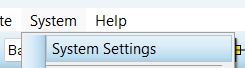
Go to the System Settings in System Tab :
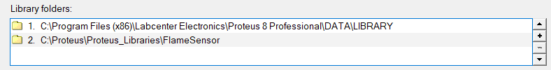
And then choose where you extract the downloaded folder :
Step 4 : Install Arduino IDE
Go and Install Arduino IDE from here : https://www.arduino.cc/en/software
2. Proteus Simulation Tutorial
Step 1 : Setup the Arduino IDE
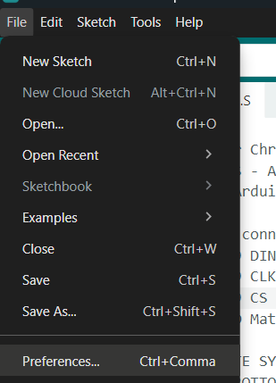
Go to Preferences :
Checklist the Show Verbose output during compile and upload :

Step 2 : Compile the Code
Compile the code using this button :

Find the Hex link on the output terminal :

Step 3 : Connect the Hex
Double click the Arduino on the Simulation :
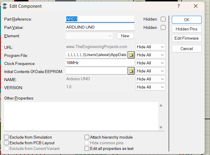
Copy the hex to the Arduino on the Proteus Simulation :
 \
\
Step 4 : Run the Code
COMPLETE
Module 2 - Introduction to AVR Assembly
1. Introduction to AVR Assembly Language
Assembly is a low-level programming language that allows manipulation of every bit in memory, resulting in highly efficient and fast code. It has a strong one-to-one correspondence with the machine code instructions of the computer architecture.
On Arduino microcontrollers (specifically the ATmega328P), Assembly programming enables high-level control suitable for real-time systems and applications requiring complex mathematical processes.
Advantages of Using Assembly:
- High efficiency: Full control over memory usage and execution time.
- Deep understanding: Helps understand fundamental microcontroller operations.
- Problem solving: Can solve problems that may arise in other high-level languages.
Disadvantages:
- Steep learning curve: Requires deep understanding of hardware architecture.
- Longer code: For simple tasks, Assembly code is much longer compared to high-level languages.
2. ATmega328P Hardware & Memory Architecture
A. Memory Map
The ATmega328P memory map provides information on how the Microcontroller Unit (MCU) uses memory. Here is the address division:
| Category | Address | Size | Description |
|---|---|---|---|
| General Purpose Registers | 0x0000 - 0x001F |
32 x 8 bit | Registers R0 - R31 |
| I/O Registers | 0x0020 - 0x005F |
64 x 8 bit | Accessible via IN/OUT instructions |
| Extended I/O Registers | 0x0060 - 0x00FF |
160 x 8 bit | Additional I/O registers |
| Internal SRAM | 0x0100 - 0x08FF |
2048 x 8 bit | Internal data memory |
B. General Purpose Working Registers (GPR)
The AVR architecture has 32 general-purpose registers labeled R0 through R31. These registers function as temporary storage for data during processing and are directly connected to the ALU (Arithmetic Logic Unit).
Register Division:
| Group | Registers | Characteristics |
|---|---|---|
| Lower Registers | R0 - R15 | Limited functionality. Cannot store immediate values directly (cannot use LDI instruction). |
| Upper Registers | R16 - R31 | More flexible. Can work with immediate data, allowing direct storage of bytes or words. |
Pointer Registers:
The last six registers (R26 through R31) can be combined into 16-bit pointers for indirect memory addressing:
| Pointer Name | Low Register | High Register | Function |
|---|---|---|---|
| X Register | R26 (XL) | R27 (XH) | Pointer for memory access |
| Y Register | R28 (YL) | R29 (YH) | Pointer for memory access |
| Z Register | R30 (ZL) | R31 (ZH) | Pointer for memory & flash access |
3. Input/Output (I/O) Programming
On the Arduino Uno (ATmega328P), digital I/O is controlled through Port B, Port C, and Port D. Each port is 8-bit, allowing control of up to 8 pins simultaneously.
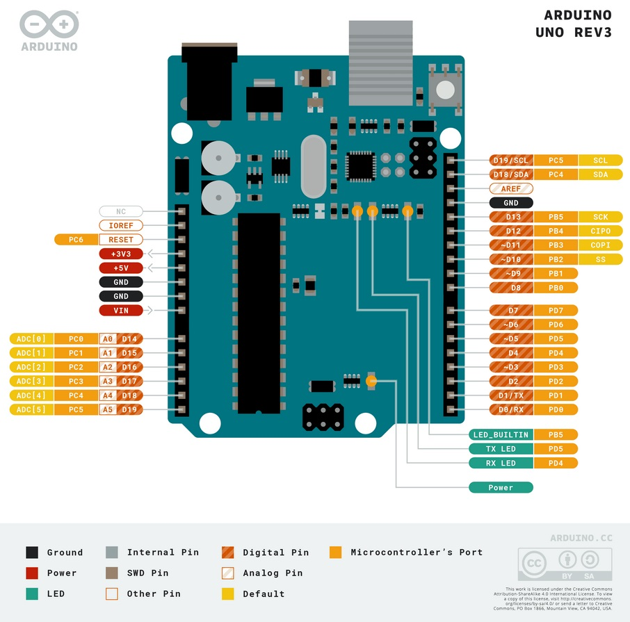
A. Port to Arduino Pin Mapping
| Port | Bits | Arduino Pin | Notes |
|---|---|---|---|
| Port B | PB0 - PB5 | Digital Pin 8 - 13 | PB6-PB7 are used for crystal oscillator |
| Port C | PC0 - PC5 | Analog Pin A0 - A5 | PC6 is the RESET pin |
| Port D | PD0 - PD7 | Digital Pin 0 - 7 | PD0 (RX) and PD1 (TX) for serial communication |
B. Main I/O Registers
Three main registers control the behavior of each port:
| Register | Full Name | Access | Function |
|---|---|---|---|
| DDRx | Data Direction Register | Read/Write | Configures pin direction. 0 = Input, 1 = Output |
| PORTx | Data Register | Read/Write | If Output: Sets logic High (1) or Low (0). If Input: Activates internal Pull-up resistor (1) or Tri-state (0) |
| PINx | Input Pins Address | Read Only | Reads the physical logic state of the pin (0 or 1) |
(Replace 'x' with Port name, e.g., DDRB, PORTB, PINB)
C. Register Bit Configuration Details
DDRx - Data Direction Register
| DDRx Bit Value | Pin Direction | Explanation |
|---|---|---|
| 0 | Input | Pin is configured as input (high impedance) |
| 1 | Output | Pin is configured as output (source/sink current) |
PORTx - Data Register (Depends on DDRx Configuration)
| DDRx | PORTx | Mode | Pin Condition |
|---|---|---|---|
| 0 (Input) | 0 | Tri-state (Hi-Z) | Pin is floating, no pull-up |
| 0 (Input) | 1 | Input Pull-up | Internal pull-up resistor active, pin defaults to HIGH |
| 1 (Output) | 0 | Output Low | Pin outputs 0V (GND) |
| 1 (Output) | 1 | Output High | Pin outputs 5V (VCC) |
PINx - Input Pins Register
| PINx Bit Value | Pin Status | Explanation |
|---|---|---|
| 0 | LOW | Pin voltage is below threshold (near 0V) |
| 1 | HIGH | Pin voltage is above threshold (near 5V) |
4. Assembly Integration with Arduino IDE
To combine Assembly with Arduino C++ code, the extern "C" directive is used in the .ino file and the .global directive is used in the .S (Assembly) file.
File Structure:
.ino File (C/C++):
extern "C" {
  void start();    // Declaration of function defined in Assembly
  void loop_asm(); // Another function from Assembly
}

void setup() {
  start();         // Call Assembly function for initialization
}

void loop() {
  loop_asm();      // Call Assembly function for main loop
}
.S File (Assembly):
#define __SFR_OFFSET 0x00
#include "avr/io.h"

.global start
.global loop_asm

start:
    SBI DDRB, 5      ; Set PB5 (Pin 13) as Output
    RET              ; Return to caller

loop_asm:
    SBI PORTB, 5     ; Turn on LED
    ; ... other code
    RET
Directive Explanations:
#define __SFR_OFFSET 0x00: Sets the offset for I/O registers to use symbolic names (DDRB, PORTB, etc.).#include "avr/io.h": Includes register definitions for the AVR chip..global: Makes label/function accessible from other files (exported symbol).RET: Instruction to return from subroutine to the calling program.
5. AVR Assembly Instruction Set
Operand Notation
Before diving into the instructions, here are the common operand symbols used:
| Symbol | Description |
|---|---|
| Rd | Destination register (R0-R31). The result of the operation is stored here. |
| Rr | Source register (R0-R31). Used as input for the operation. |
| K | Constant/Immediate value (8-bit: 0-255 or 0x00-0xFF). |
| k | Address constant for SRAM or program memory. |
| A | I/O register address (0-63 for IN/OUT, 0-31 for SBI/CBI). |
| b | Bit number (0-7) within a register or I/O address. |
| X, Y, Z | Pointer registers (X=R27:R26, Y=R29:R28, Z=R31:R30). |
Note: Some instructions only work with upper registers (R16-R31), such as LDI, ANDI, ORI, SUBI, SBCI, and CPI.
A. Data Transfer Instructions
Used to move data between registers or between registers and memory/I/O.
| Mnemonic | Operand | Description | Example | Notes |
|---|---|---|---|---|
| LDI | Rd, K | Load Immediate | LDI R16, 0xFF |
Loads 8-bit constant K into register Rd (R16-R31 only) |
| MOV | Rd, Rr | Move/Copy Register | MOV R0, R1 |
Copies contents of register Rr to Rd |
| IN | Rd, A | Input from I/O | IN R16, PINB |
Reads data from I/O port A to register Rd |
| OUT | A, Rr | Output to I/O | OUT PORTB, R16 |
Sends data from register Rr to I/O port A |
| LDS | Rd, k | Load from SRAM | LDS R16, 0x0100 |
Loads data from SRAM address k to register Rd |
| STS | k, Rr | Store to SRAM | STS 0x0100, R16 |
Stores register Rr contents to SRAM address k |
| LD | Rd, X/Y/Z | Load Indirect | LD R16, X |
Loads data from address pointed by pointer X/Y/Z |
| ST | X/Y/Z, Rr | Store Indirect | ST X, R16 |
Stores data to address pointed by pointer X/Y/Z |
| PUSH | Rr | Push to Stack | PUSH R16 |
Saves register to stack |
| POP | Rd | Pop from Stack | POP R16 |
Retrieves data from stack to register |
B. Bit Manipulation Instructions (I/O Specific)
These instructions operate on the lower 32 I/O addresses ($00-$1F). Very efficient for changing one bit without affecting other bits.
| Mnemonic | Operand | Description | Example | Notes |
|---|---|---|---|---|
| SBI | A, b | Set Bit in I/O | SBI DDRB, 5 |
Sets bit b in I/O register A to 1 |
| CBI | A, b | Clear Bit in I/O | CBI PORTB, 5 |
Clears bit b in I/O register A to 0 |
| BST | Rr, b | Bit Store to T | BST R16, 3 |
Copies bit b from register Rr to T flag |
| BLD | Rd, b | Bit Load from T | BLD R17, 5 |
Copies T flag to bit b of register Rd |
C. Arithmetic Instructions
| Mnemonic | Operand | Description | Example | Notes |
|---|---|---|---|---|
| ADD | Rd, Rr | Add | ADD R1, R2 |
Rd = Rd + Rr |
| ADC | Rd, Rr | Add with Carry | ADC R1, R2 |
Rd = Rd + Rr + C (Carry flag) |
| SUB | Rd, Rr | Subtract | SUB R16, R17 |
Rd = Rd - Rr |
| SBC | Rd, Rr | Subtract with Carry | SBC R16, R17 |
Rd = Rd - Rr - C |
| SUBI | Rd, K | Subtract Immediate | SUBI R16, 10 |
Rd = Rd - K (R16-R31 only) |
| SBCI | Rd, K | Subtract Immediate with Carry | SBCI R17, 0 |
Rd = Rd - K - C |
| INC | Rd | Increment | INC R16 |
Rd = Rd + 1 |
| DEC | Rd | Decrement | DEC R16 |
Rd = Rd - 1 |
| MUL | Rd, Rr | Multiply Unsigned | MUL R16, R17 |
R1:R0 = Rd × Rr (16-bit result) |
| MULS | Rd, Rr | Multiply Signed | MULS R16, R17 |
R1:R0 = Rd × Rr (signed) |
| NEG | Rd | Negate (Two's Complement) | NEG R16 |
Rd = 0x00 - Rd |
D. Logic Instructions
| Mnemonic | Operand | Description | Example | Notes |
|---|---|---|---|---|
| AND | Rd, Rr | Logical AND | AND R1, R2 |
Rd = Rd AND Rr |
| ANDI | Rd, K | AND Immediate | ANDI R16, 0x0F |
Rd = Rd AND K (masking) |
| OR | Rd, Rr | Logical OR | OR R1, R2 |
Rd = Rd OR Rr |
| ORI | Rd, K | OR Immediate | ORI R16, 0x80 |
Rd = Rd OR K |
| EOR | Rd, Rr | Exclusive OR | EOR R16, R17 |
Rd = Rd XOR Rr |
| COM | Rd | One's Complement | COM R16 |
Rd = 0xFF - Rd (inverts all bits) |
| CLR | Rd | Clear Register | CLR R16 |
Rd = 0 (same as EOR Rd, Rd) |
| SER | Rd | Set Register | SER R16 |
Rd = 0xFF (R16-R31 only) |
E. Shift & Rotate Instructions
| Mnemonic | Operand | Description | Example | Notes |
|---|---|---|---|---|
| LSL | Rd | Logical Shift Left | LSL R16 |
Shift left, bit 0 = 0, bit 7 → Carry |
| LSR | Rd | Logical Shift Right | LSR R16 |
Shift right, bit 7 = 0, bit 0 → Carry |
| ROL | Rd | Rotate Left through Carry | ROL R16 |
Rotate left through Carry flag |
| ROR | Rd | Rotate Right through Carry | ROR R16 |
Rotate right through Carry flag |
| ASR | Rd | Arithmetic Shift Right | ASR R16 |
Shift right, bit 7 remains (preserve sign) |
| SWAP | Rd | Swap Nibbles | SWAP R16 |
Swaps upper and lower 4-bits in register |
F. Branch & Control Flow Instructions
| Mnemonic | Operand | Description | Example | Notes |
|---|---|---|---|---|
| RJMP | k | Relative Jump | RJMP loop |
Jump to label k (±2K words) |
| JMP | k | Jump | JMP far_label |
Jump to 22-bit address (all memory) |
| RCALL | k | Relative Call | RCALL delay |
Call subroutine relative to PC |
| CALL | k | Call | CALL far_sub |
Call subroutine at 22-bit address |
| RET | - | Return | RET |
Return from subroutine |
| RETI | - | Return from Interrupt | RETI |
Return from interrupt handler |
| CP | Rd, Rr | Compare | CP R16, R17 |
Compare Rd with Rr (updates flags) |
| CPI | Rd, K | Compare Immediate | CPI R16, 5 |
Compare Rd with constant K |
| CPC | Rd, Rr | Compare with Carry | CPC R17, R19 |
For multi-byte comparison |
| BREQ | k | Branch if Equal | BREQ target |
Jump if Z flag = 1 (result equal) |
| BRNE | k | Branch if Not Equal | BRNE loop |
Jump if Z flag = 0 (result not equal) |
| BRLO | k | Branch if Lower | BRLO less |
Jump if C flag = 1 (unsigned <) |
| BRSH | k | Branch if Same or Higher | BRSH greater |
Jump if C flag = 0 (unsigned ≥) |
| BRLT | k | Branch if Less Than | BRLT neg |
Jump if S flag = 1 (signed <) |
| BRGE | k | Branch if Greater or Equal | BRGE pos |
Jump if S flag = 0 (signed ≥) |
G. Skip Instructions
| Mnemonic | Operand | Description | Example | Notes |
|---|---|---|---|---|
| SBIS | A, b | Skip if Bit in I/O Set | SBIS PINB, 0 |
Skip next instruction if bit = 1 |
| SBIC | A, b | Skip if Bit in I/O Cleared | SBIC PIND, 2 |
Skip next instruction if bit = 0 |
| SBRS | Rr, b | Skip if Bit in Register Set | SBRS R16, 7 |
Skip if bit b in register = 1 |
| SBRC | Rr, b | Skip if Bit in Register Cleared | SBRC R16, 0 |
Skip if bit b in register = 0 |
H. Other Instructions
| Mnemonic | Operand | Description | Example | Notes |
|---|---|---|---|---|
| NOP | - | No Operation | NOP |
Does nothing (1 clock cycle) |
| SLEEP | - | Sleep | SLEEP |
Enters sleep mode (power saving) |
| WDR | - | Watchdog Reset | WDR |
Resets watchdog timer |
| SBIW | Rd, K | Subtract Immediate from Word | SBIW R24, 1 |
Subtract K from 16-bit value (R25:R24) |
| ADIW | Rd, K | Add Immediate to Word | ADIW R24, 1 |
Add K to 16-bit value |
6. Status Register (SREG)
The Status Register contains flags that indicate the results of arithmetic/logic operations. This register is crucial for branch instructions.
| Bit | Name | Description |
|---|---|---|
| 7 | I (Global Interrupt Enable) | Enables/disables global interrupts |
| 6 | T (Bit Copy Storage) | Storage for BLD/BST instructions |
| 5 | H (Half Carry Flag) | Carry from bit 3 to bit 4 (for BCD) |
| 4 | S (Sign Flag) | S = N ⊕ V (for signed operations) |
| 3 | V (Overflow Flag) | Two's complement overflow |
| 2 | N (Negative Flag) | Result is negative (bit 7 = 1) |
| 1 | Z (Zero Flag) | Result = 0 |
| 0 | C (Carry Flag) | Carry/borrow from operation |
7. Delay Implementation Without Library
Delays can be created using nested loops that consume a certain number of clock cycles.
Delay Calculation Concept:
- ATmega328P on Arduino Uno runs at 16 MHz (16 million clock cycles per second)
- 1 millisecond = 16,000 clock cycles
DECinstruction takes 1 cycle,BRNEtakes 2 cycles (if branch taken)
Delay Implementation Examples:
; Delay approximately 1 second (with nested loop)
delay_1s:
    LDI R18, 64          ; Outer counter
outer_loop:
    LDI R24, lo8(62500)  ; Inner counter low byte
    LDI R25, hi8(62500)  ; Inner counter high byte
inner_loop:
    SBIW R24, 1          ; Subtract 16-bit counter (2 cycles)
    BRNE inner_loop      ; Loop if not 0 (2 cycles if taken)
    DEC R18              ; Subtract outer counter
    BRNE outer_loop      ; Loop outer if not 0
    RET

; Simple delay with single loop
delay_simple:
    LDI R16, 255         ; Load counter
delay_loop:
    DEC R16              ; Decrement counter (1 cycle)
    BRNE delay_loop      ; Branch if not zero (2 cycles)
    RET                  ; Return (approximately 765 cycles total)
8. Complete Program Examples
A. Blink LED
#define __SFR_OFFSET 0x00
#include "avr/io.h"

.global main

main:
    SBI DDRB, 5          ; Set PB5 (Pin 13) as Output

loop:
    SBI PORTB, 5         ; Turn on LED (Output HIGH)
    RCALL delay          ; Call delay subroutine
    CBI PORTB, 5         ; Turn off LED (Output LOW)
    RCALL delay          ; Call delay subroutine
    RJMP loop            ; Repeat continuously

delay:
    LDI R18, 82          ; Outer loop counter
outer:
    LDI R24, lo8(60000)  ; Inner loop counter (low byte)
    LDI R25, hi8(60000)  ; Inner loop counter (high byte)
inner:
    SBIW R24, 1          ; Subtract word (R25:R24)
    BRNE inner           ; Loop if not 0
    DEC R18              ; Subtract outer counter
    BRNE outer           ; Loop outer if not 0
    RET                  ; Return to caller
B. Reading Button and Controlling LED
#define __SFR_OFFSET 0x00
#include "avr/io.h"

.global main

main:
    ; Setup
    SBI DDRB, 5          ; PB5 (Pin 13) as Output (LED)
    CBI DDRD, 2          ; PD2 (Pin 2) as Input (Button)
    SBI PORTD, 2         ; Activate Pull-up on PD2

loop:
    SBIC PIND, 2         ; Skip next instruction if button pressed (LOW)
    RJMP led_off         ; If not pressed, turn off LED

led_on:
    SBI PORTB, 5         ; Turn on LED
    RJMP loop            ; Return to loop

led_off:
    CBI PORTB, 5         ; Turn off LED
    RJMP loop            ; Return to loop
C. Toggle LED with Button (Simple Debounce)
#define __SFR_OFFSET 0x00
#include "avr/io.h"

.global main

main:
    ; Initialization
    SBI DDRB, 5          ; PB5 as Output (LED)
    CBI DDRD, 2          ; PD2 as Input (Button)
    SBI PORTD, 2         ; Activate internal Pull-up
    CLR R20              ; R20 = LED status (0 = off)

wait_press:
    SBIC PIND, 2         ; Wait for button pressed (LOW)
    RJMP wait_press

    ; Button pressed - toggle LED
    SBRC R20, 0          ; Skip if bit 0 of R20 = 0 (LED off)
    RJMP turn_off

turn_on:
    SBI PORTB, 5         ; Turn on LED
    LDI R20, 1           ; Set status = on
    RJMP debounce

turn_off:
    CBI PORTB, 5         ; Turn off LED
    CLR R20              ; Set status = off

debounce:
    RCALL delay          ; Delay for debounce

wait_release:
    SBIS PIND, 2         ; Wait for button released (HIGH)
    RJMP wait_release
    RCALL delay          ; Delay debounce after release
    RJMP wait_press      ; Return to wait for press

delay:
    LDI R18, 50
d_outer:
    LDI R24, lo8(10000)
    LDI R25, hi8(10000)
d_inner:
    SBIW R24, 1
    BRNE d_inner
    DEC R18
    BRNE d_outer
    RET
Module 3 - Serial Port
Introduction to USART
1. USART Definition
USART (Universal Synchronous/Asynchronous Receiver/Transmitter) is a communication protocol used to transfer data between electronic devices, such as microcontrollers, sensors, and other components. This protocol is highly flexible as it supports two main modes:
- Synchronous
- Asynchronous
2. UART vs. USART
While often used interchangeably, there is a technical difference:
- UART (Universal Asynchronous Receiver/Transmitter): Supports only asynchronous communication. It requires no clock signal as it relies on start/stop bits and pre-defined baud rates.
- USART (Universal Synchronous/Asynchronous Receiver/Transmitter): A superset of UART. It supports both asynchronous and synchronous modes. In synchronous mode, a dedicated clock pin (XCK) is used to synchronize data.
3. Operating Modes
A. Asynchronous Mode
In this mode, the USART module transmits data without an external clock signal. Synchronization is achieved using data frames consisting of:
- Start Bit: Indicates the beginning of transmission.
- Data Bits: Contains the primary information (typically 5-9 bits).
- Parity Bit (Optional): Used for error detection (Even, Odd, or None).
- Stop Bit: Indicates the end of transmission.
Characteristics: Suitable for long-distance communication or between devices that do not share the same clock.
B. Synchronous Mode
Uses a clock signal to synchronize data transfer between the transmitter and the receiver.
- Requires the same clock configuration on both devices.
- Allows for faster and more reliable data transfer compared to asynchronous mode.
Characteristics: Ideal for multimedia applications or high-speed bulk data transfers.
4. Configuration and Baud Rate
To use USART, several parameters must be defined:
- Baud Rate: The speed of data transmission (bits per second).
- Data Format: The number of data bits, parity, and stop bits.
- Interrupt: Enables notifications when data is finished being sent or received.
5. USART and Arduino Serial Monitor
In the Arduino ecosystem (such as the Uno), the USART peripheral is the primary way the microcontroller communicates with your computer:
- Hardware Connection: The ATmega328P uses its USART pins (TX on Pin 1, RX on Pin 0). These are connected to an onboard USB-to-Serial converter chip.
- Serial Monitor: When you open the Serial Monitor or Serial Plotter in the Arduino IDE, it acts as the "Receiver" (RX) for data sent by the Arduino and the "Transmitter" (TX) for data you type in.
- Baud Rate Alignment: For communication to work, the baud rate selected in the Serial Monitor (e.g., 9600) must match the baud rate configured in your code. If they do not match, you will see "garbage" characters or no data at all.
In Proteus, follow these steps to simulate using a Virtual Terminal to mimic Serial Monitor functionality:
- Click on Virtual Instruments Mode in the left sidebar.

- Select the Virtual Terminal component and place it on the schematic.

- Add an Arduino Uno to your schematic. Then, connect the TX and RX pins of the Virtual Terminal to the RX and TX pins of the Arduino Uno respectively.

- Double-click on the Virtual Terminal to set the Baud Rate (e.g., 9600) to match your code.

Baud Rate Calculation Formula (UBRR)
The UBRR (USART Baud Rate Register) value is calculated based on the CPU clock frequency (F_CPU) and the desired Baud Rate:
UBRR = (F_CPU / (16 * BAUD)) - 1
Calculation Example:
If F_CPU = 16 MHz and the target BAUD = 9600 bps:
- UBRR = (16,000,000 / (16 * 9600)) - 1
- UBRR = 104.16 - 1
- UBRR ≈ 103 (Hex: 0x67)
USART Register Architecture of ATmega328p
The ATmega328p microcontroller uses several specific registers to control and monitor USART communication.
1. UBRR (USART Baud Rate Register)

A 16-bit register that determines the communication speed. It is divided into two 8-bit registers:
- UBRR0H: Stores the 8 most significant bits (MSB).
- UBRR0L: Stores the 8 least significant bits (LSB).
The following table provides a reference for UBRR0 (USART Baud Rate Register) settings corresponding to standard baud rates (bps). It details the required register values for three common oscillator frequencies (f_osc): 16.0000 MHz, 18.4320 MHz, and 20.0000 MHz. For each frequency, the table accounts for both normal speed (U2Xn = 0) and double speed (U2Xn = 1) modes, including the resulting percentage error for each configuration.

2. UDR (USART Data Register)

An 8-bit register that serves a dual purpose:
- TXB (Transmit Data Buffer): The location where data to be sent is written.
- RXB (Receive Data Buffer): The location where incoming data is read.
3. UCSR0A (USART Control and Status Register A)

Used to monitor communication status and configure the speed mode.
| Bit | Name | Description |
|---|---|---|
| RXC0 | Receive Complete | Set to 1 if there is new unread data in the UDR. |
| TXC0 | Transmit Complete | Set to 1 if all data has been transmitted. |
| UDRE0 | UDR Empty | Set to 1 if the UDR register is empty and ready for new data. |
| FE0 | Frame Error | Occurs when there is an error in the stop bit. |
| DOR0 | Data Overrun | Occurs when new data arrives before old data is read. |
| UPE0 | Parity Error | Occurs when there is a parity error in the received data. |
| U2X0 | Double Speed | If set to 1, the transmission speed is doubled. |
| MPCM0 | Multi-processor | Enables multi-processor communication mode. |
4. UCSR0B (USART Control and Status Register B)

Used to enable the module and interrupts.
- RXCIE0: Enables the receive complete interrupt.
- TXCIE0: Enables the transmit complete interrupt.
- UDRIE0: Enables the data register empty interrupt.
- RXEN0: Enables the Receiver.
- TXEN0: Enables the Transmitter.
- UCSZ02: Additional bit (along with UCSR0C) to determine data size (5-9 bits).
- RXB80 / TXB80: Holds the 9th data bit (if using 9-bit format).
5. UCSR0C (USART Control and Status Register C)

Used for frame format configuration and operating mode.
- UMSEL01:0: Selects the mode (Asynchronous or Synchronous).
- UPM01:0: Selects the Parity mode (None, Even, or Odd).
- USBS0: Selects the number of Stop Bits (1 or 2).
- UCSZ01:0: Determines the data size (paired with UCSZ02 in UCSR0B).
- UCPOL0: Clock polarity for synchronous mode.
Note: When writing to UCSR0C, ensure bit configurations are performed carefully according to the communication protocol requirements of the target device.
Implementation and Assembly Code Examples
This page contains basic implementation examples of USART serial communication using the Assembly programming language on an AVR Microcontroller (ATmega328p).
1. Printing Text to Serial Monitor
This code is used to repeatedly send the string "Programming Serial Interface!" to the Serial Monitor via the USART port.
;------------------------
; Assembly Code - Print Text
;------------------------
#define __SFR_OFFSET 0x00
#include "avr/io.h"
;------------------------
.global main

main:
    CLR   R24
    STS   UCSR0A, R24               ; Clear UCSR0A register
    STS   UBRR0H, R24               ; Clear UBRR0H
    LDI   R24, 103                  ; Set UBRR value = 103 (9600 Baud Rate)
    STS   UBRR0L, R24

    LDI   R24, (1<<RXEN0) | (1<<TXEN0) ; Enable RX and TX
    STS   UCSR0B, R24

    LDI   R24, (1<<UCSZ00) | (1<<UCSZ01) ; Mode: 8-bit data, 1 stop bit, No Parity
    STS   UCSR0C, R24

print_msg:
    LDI   R30, lo8(message)
    LDI   R31, hi8(message)         ; Z points to string message
agn:
    LPM   R18, Z+                   ; Load character into R18
    CPI   R18, 0                    ; Check if end of string (null)
    BREQ  ext                       ; If yes, exit loop

l1:
    LDS   R17, UCSR0A
    SBRS  R17, UDRE0                ; Wait until buffer is empty (UDRE0=1)
    RJMP  l1
    STS   UDR0, R18                 ; Send character to Serial Monitor
    RJMP  agn                       ; Loop to next character

ext:
    RCALL delay_sec                 ; Wait for a moment
    RJMP  print_msg                 ; Repeat string transmission

message:
    .ascii "Programming Serial Interface!"
    .byte 10, 13, 0

delay_sec:                          ; Delay Subroutine (~3 seconds)
    LDI   R20, 255
l4: LDI   R21, 255
l5: LDI   R22, 255
l6: DEC   R22
    BRNE  l6
    DEC   R21
    BRNE  l5
    DEC   R20
    BRNE  l4
    RET
2. Reading Input from Serial Monitor
This code reads characters sent from the Serial Monitor and controls an LED. If the character 'H' is received, the LED turns ON; if 'L' is received, the LED turns OFF.
;------------------------
; Assembly Code - Input Text and Control LED
;------------------------
#define __SFR_OFFSET 0x00
#include "avr/io.h"
;------------------------
.global main

main:
    CLR   R24
    STS   UBRR0H, R24
    LDI   R24, 103
    STS   UBRR0L, R24
    LDI   R24, (1<<RXEN0 | 1<<TXEN0)
    STS   UCSR0B, R24
    LDI   R24, (1<<UCSZ01 | 1<<UCSZ00)
    STS   UCSR0C, R24

    SBI   DDRB, 5               ; Set PB5 as output

wait_input:
    ; 1. Check if a byte arrived
    LDS   R17, UCSR0A
    SBRS  R17, RXC0             ; Wait for Receive Complete
    RJMP  wait_input

    ; 2. Read the character into R18
    LDS   R18, UDR0

    ; 3. Check if character is 'H'
    CPI   R18, 'H'
    BREQ  led_on

    ; 4. Check if character is 'L'
    CPI   R18, 'L'
    BREQ  led_off

    RJMP  wait_input

led_on:
    SBI   PORTB, 5              ; Turn LED ON
    RJMP  wait_input

led_off:
    CBI   PORTB, 5              ; Turn LED OFF
    RJMP  wait_input
Module 4 - Arithmetic
From memory access, addressing modes, the SREG, to arithmetic operations in AVR assembly,
1. Memory in AVR Architecture
AVR Architecture is an 8 bit single-chip RISC microcontroller with a modified Harvard Architecture that is organized as the following which causes it to behave certain ways when handling memory.

You don't have to memorize all this don't worry.
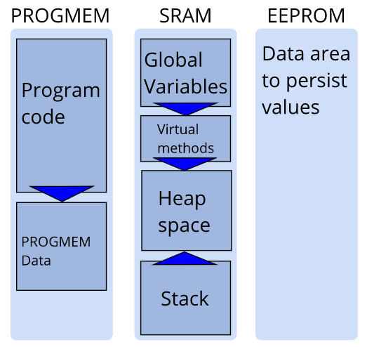
There are several memory spaces in this organization, but for now we will look at the two most important ones to know.
Program/Flash Memory
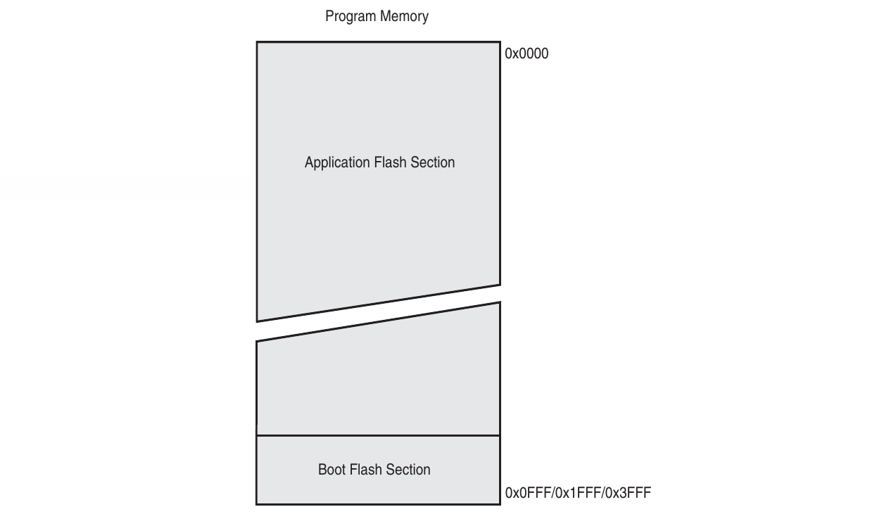 When you compile and upload codes (flashing), it's stored in the Flash Memory section semi-permanently. During runtime, the control unit fetches instructions from this memory section.
This portion of the memory is non-volatile which means the data stored won't be erased after power loss.
Data Memory - DS (Data Space)
 The Data Memory consists of several memory parts mapped into one contiguous memory addresses.
- 32 General Purpose Registers (0x0000 - 0x001F)
- 64 I/O Registers (0x0020 - 0x005F)
- 160 Extended I/O Registers (0x0060 - 0x00FF)
- SRAM (Implementation Spesific)
The Static RAM (SRAM) is a memory block used to store data used during runtime. One part of this is the stack that may come in handy for temporary data (more on this later).
2. Addressing Modes
Due to how the AVR Architecture and its memory are organized, AVR instructions, including arithmetic instructions, must follow certain addressing methods. Addressing methods are how the control unit may access different data locations according to the instruction which are usually 16 - 32 bits in length. Those data locations may include general purpose registers, I/O registers, extended I/O registers, and the SRAM.
Single Register Direct (Rd)

Operates on a single general purpose register Rd with d being values 0 - 31 (R0 - R31). Data is read from the register Rd, operated on, then stored back into the same register.
Some instructions with this addressing mode are ROL Rd and COM Rd which rotates the bits in Rd and inverts the bits in Rd respectively.
Double Register Direct (Rd, Rr)

Unlike Single Register Direct, Double Register Direct operates on two general purpose registers: source Rr and destination Rd. Data is read from Rr which are then operated alongside Rd to be stored back into Rd.
Instructions such as ADD Rd, Rr and AND Rd, Rr operates on both Rd and Rr which then stores the results (Addition and bitwise AND) in Rd.
Immediate Mode (Rd, K)
A constant value K alongside a register Rd is provided in the instruction itself, therefore the data itself is stored as a constant inside the Flash Memory. The constant value is limited to 255 (0xFF, 8 bits) and the register used is limited to R16 - R31 (4 bits with an offset).
Instructions such as ORI Rd, K and LDI Rd, K operates with a constant value K then storing it into Rd (bitwise OR and Loading).
Notice how the instructions have 'I' in its names (stands for Immediate).
Some instructions that have W (Word) in its name operates on 16 bit words which are stored in two consecutive registers R[d + 1]:Rd. One instruction that operates like this is the ADIW Rd, K that adds a constant K to the 16 bit data in R[d + 1]:Rd. Word Immediate instructions can only operate on 4 even-indexed GP registers {R24, R26, R28, R30} and are limited to 6 bits constant values (0 - 63).
The 16 bit opcode for ADIW is [1001 0110 KKdd KKK] which limits K to 6 bits and d to 2 bits (4 different registers max).
I/O Direct (Rd/Rr, A)

Operates with I/O memory address A. Headers like avr/io.h defines these memory addresses into readable constants such as PORTB, PINC, and 'DDRA'. This doesn't include Extended I/O addresses such as UBBR0H.
Instructions such as IN Rd, A and OUT A, Rr stores IO(A) into Rd and Rr into IO(A) respectively.
Data Direct (Rd/Rr, k)
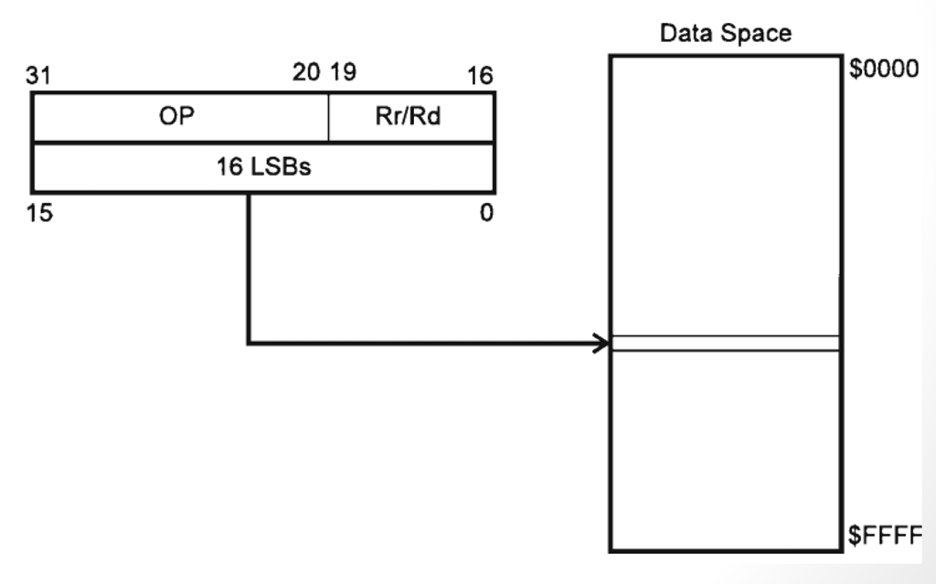
Instructions with this addressing utilizes 16 bit value k (0 - 65535) which is an address that corresponds to a space in memory, including the Extended I/O addresses scuh as UBRR0H and UCSR0A.
One instruction with Data Direct addressing is LDS Rd, k which loads the value in address k to register Rd.
Data Indirect (Rd/Rr, X/Y/Z +/- q)
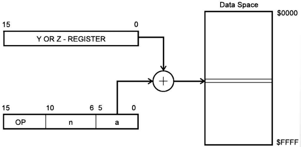
Registers X, Y, and Z corresponds to certain 16 bit register pairs in the memory.
| Register | Higher Byte | Lower Byte |
|---|---|---|
| X | R27 | R26 |
| Y | R29 | R28 |
| Z | R31 | R30 |
Instructions with Data Indirect addressing operates on data stored in the address stored in the X/Y/Z registers. For example, if X contains the value 0x01FF, then LD Rd, X would load the data value stored in address 0x01FF into Rd.
A feature of Data Indirect addressing is pre/post increment/decrement operators. By adding '+' or '-' next to the X/Y/Z register (eg: X+), the address stored would be automatically incremented or decremented respectively. This operation can be pre-ordered or post-ordered meaning the address value change would happen before or after the instruction itself.
As an example, assume Y = 0x02. Instruction LD Rd, Y+ would store the value DS(Y) into Rd THEN increments Y to be 0x03. As opposed to this, putting the increment operator before Y (LD Rd, +Y) would first increment the value of Y to be 0x03 THEN loads the data in the newly updated address into Rd.
This may come in handy when operating with arrays stored as blocks of consecutive memory.
Certain instructions also allows accessing memory with displacement q on pointer registers Y/Z (X gak diajak). These instructions, usually ending with D, such as STD Y+3, Rd would offset the address stored in Y by 3 which stores the value in Rd into address DS(Y+3).
To see which instructions uses which memory addressing methods, refer to the AVR Instruction Set Manual. Knowing which instructions utilizes which memory addressing method would help you choose the best instruction to use in different situations when handling arithmetic and logic operations.
3. The Status Register
The Status Register (SREG) is a special 8 bit register that saves different operational status flags in each bit. Different operations may affect different flags (bit) of the register which then would be useful to create decisions after.
In AVR architecture, SREG is an I/O register meaning that it can be operated with instructions such as OUT and IN.

Carry Flag (C) [0]
- Indicates a Carry after addition or a Borrow after substraction.
- Usually happens when adding up numbers that results in a result greater than 8 bits (255) or when substracting numbers that results a negative analytically.
- Substracting a smaller number by a bigger one would result to a negative. This can be used to test whether a number is smaller than the other.
Zero Flag (Z) [1]
- Indicates that the previous operation results a 0.
- Can be set by different arithmetic operations such as
SUBorDECto logical operations such asAND. - Substracting two equal values would result in a 0. This property can be used to test if two numbers are equal.
Negative Flag (N) [2]
- Indicates that the previous number results a negative.
- Under the hood works by testing the most significant bit (bit 7, leftmost) which indicates a 2s complement.
Two's Complement Overflow Flag (V) [3]
- Indicates that the previous operation is outside the range of signed values -128 to 127. These two values are the lowest and highest 8 bit signed values.
- Useful for testing overflow during signed 8 bit integer operations.
Sign Flag (S) [4]
- XOR of N and V flag.
- Indicates the sign of the result of the last operation. S = 1 means the last operation resulted in a negative signed number.
Half Carry (H) [5]
- Functions like the Carry flag but for only the lower nibbles of the last operation.
- Can come in handy when operating with 4 bit values such as BCD.
Bit Copy Storage (T) [6]
- Unlike the others, can be freely used by the programmer anyway they like.
- Set to 1 with
SETand 0 withCLTinstructions. - Can be used by other registers with
BST Rr, bandBLD Rd, bthat moves the 1 bit value of T into or out of bit b of register Rr/Rd. - Technically a free 1 bit storage.
Global Interrupt Enable (I) [7]
- Enables interrupt when set to 1 with
SEIor disables it when cleared withCLI.
4. Advanced Arithmetic Operations
As a refresher, here are some fundamental AVR arithmetic and logical instructions.
| Mnemonic | Operand | Description | Example | Notes |
|---|---|---|---|---|
| ADD | Rd, Rr | Add | ADD R1, R2 |
Rd = Rd + Rr |
| ADC | Rd, Rr | Add with Carry | ADC R1, R2 |
Rd = Rd + Rr + C (Carry flag) |
| ADIW | Rd, K | Add Immediate to Word | ADIW R24, 40 |
R[d+1]:Rd = R[d+1]:Rd + K |
| SUB | Rd, Rr | Subtract | SUB R16, R17 |
Rd = Rd - Rr |
| SBC | Rd, Rr | Subtract with Carry | SBC R16, R17 |
Rd = Rd - Rr - C |
| SUBI | Rd, K | Subtract Immediate | SUBI R16, 67 |
Rd = Rd - K |
| SBIW | Rd, K | Substract Immediate from Word | SBIW R24, 40 |
R[d+1]:Rd = R[d+1]:Rd - K |
| SBCI | Rd, K | Subtract Immediate with Carry | SBCI R17, 0 |
Rd = Rd - K - C |
| INC | Rd | Increment | INC R16 |
Rd = Rd + 1 |
| DEC | Rd | Decrement | DEC R16 |
Rd = Rd - 1 |
| MUL | Rd, Rr | Multiply Unsigned | MUL R16, R17 |
R1:R0 = Rd × Rr (16-bit result) |
| MULS | Rd, Rr | Multiply Signed | MULS R16, R17 |
R1:R0 = Rd × Rr (signed) |
| NEG | Rd | Negate (Two's Complement) | NEG R16 |
Rd = 0x00 - Rd |
| AND | Rd, Rr | Logical AND | AND R1, R2 |
Rd = Rd AND Rr |
| ANDI | Rd, K | AND Immediate | ANDI R16, 0x0F |
Rd = Rd AND K |
| OR | Rd, Rr | Logical OR | OR R1, R2 |
Rd = Rd OR Rr |
| ORI | Rd, K | OR Immediate | ORI R16, 0x80 |
Rd = Rd OR K |
| EOR | Rd, Rr | Exclusive OR | EOR R16, R17 |
Rd = Rd XOR Rr |
| COM | Rd | One's Complement | COM R16 |
Rd = 0xFF - Rd (inverts all bits) |
| NEG | Rd | Two's Complement | NEG R16 |
Rd = -Rd (Signed) |
| CLR | Rd | Clear Register | CLR R16 |
Rd = 0 |
| SER | Rd | Set Register | SER R16 |
Rd = 0xFF (R16-R31 only) |
Register Pair Arithmetic
To perform arithmetic operations with 16 bit words (0 - 65535), we can utilize the Carry Flag to perform ripple carry arithmetic operations.
16 Bit Word Addition
Suppose you want to add two big 16 bit numbers 26983 and 4882 stored in two register pairs R16:R17 and R18:R19. You can add the lower byte first then add the higher byte with a carry addition.
; DEC 26983 = HEX 0x6967
LDI R16, 0x69   ; upper byte
LDI R17, 0x67   ; lower byte

; DEC 4882 = HEX 0x1312
LDI R18, 0x13   ; upper byte
LDI R19, 0x12   ; lower byte

ADD R17, R19    ; add lower byte
ADC R16, R18    ; add upper byte + carry from lower

; R16:R17 = 31865
16 Bit Word Substraction
A similar thing can be done for substracting two 16 bit numbers.
; DEC 26983 = HEX 0x6967
LDI R16, 0x69   ; upper byte
LDI R17, 0x67   ; lower byte

; DEC 4882 = HEX 0x1312
LDI R18, 0x13   ; upper byte
LDI R19, 0x12   ; lower byte

SUB R17, R19    ; substract lower byte
SBC R16, R18    ; substract upper byte - borrow (C) from lower

; R16:R17 = 22101
Immediate Arithmetic
There are 3 immediate arithmetic instructions: ADIW, SBIW, and SUBI. In AVR there is no "Add with immediate" instruction. To do so, you can utilize the SUBI Rd, K instruction to substract a negative immediate number to achieve addition.
Suppose you want to add 67 to 61 stored in R16. You can do the following
LDI     R16, 61
SUBI    R16, -67 ; - -61 = + 61
; R16 = 128
Notice how there are only immediate instructions for word addition and substraction? Recall that word immediate addressing (ADIW & SBIW) can only operate on 6 bit values (0 - 63). How can we perform immediate arithmetic operations on bigger numbers like 26983?
Word Immediate Arithmetic
To perform addition/substraction operation with immediate numbers greater than 63, we simply split the word operation into two byte immediate operations similar to the previously explained 16 bit operations.
16 Bit Immediate Addition
; DEC 4882 = HEX 0x1312
LDI R16, 0x13       ; upper byte
LDI R17, 0x12       ; lower byte

.EQU num, 0x5457    ; immediate constant DEC 21591
SUBI R17, lo8(-num) ; 0x12 - -0x57 = 0x12 + 0x57         ; add lower byte
SBCI R16, hi8(-num) ; 0x13 - -0x54 - C = 0x13 + 0x54 + C ; add upper byte
; R16:R17 = 26473
16 Bit Immediate Substraction
LDI R16, 0x67       ; yeah you get the idea atp
LDI R17, 0x69

.EQU num, 0x1312
SUBI R17, lo8(num)  ; this time we simply just substract it
SBCI R16, hi8(num)  ; no need to be negative :)
; R16:R17 = 26983
Multiplying Numbers
There are multiple multiplication instructions in AVR, each supporting different data formats such as MUL Rd, Rr for unsigned numbers, MULS Rd, Rr for signed numbers, and MULSU Rd, Rr for multiplying a signed with an unsigned number.
Generally, the way they behave are similar: they multiply Rd with Rr then storing a 16 bit result in R1:R0.
LDI R16, 23
LDI R17, 9
MUL R16, R17
; R1:R0 = 23 * 9 = 207 (16 bits wide)
5. The Stack
The Stack is a memory section of the SRAM that follows First-In-First-Out (FIFO) principles. It is generally used to store temporary data for quick and easy access.
The top of the stack is tracked by the 16 bit (adjusting to memory addressing) Stack Pointer that stores the address. It increments and decrements accordingly.

The stack grows downwards meaning that newer data is placed on lower memory address.
The top, is in fact, the bottom
The stack is used during subroutine (think of functions) calling to store the previous program counter when called with RCALL or ICALL. The program then restores the program counter to return to the previous location with RET.
Aside from subroutines, you can utilize the stack for your own use. The following are instructions that affects the stack.
| Instruction | Stack Pointer | Description |
|---|---|---|
| PUSH Rd | SP = SP - 1 | Value in Rd is pushed onto the top of the stack. |
| POP Rr | SP = SP + 1 | The top of the stack is popped into Rr |
| RCALL ICALL | SP = SP - 2 | PC is stored onto the stack. Program jumps to the subroutine. |
| RET RETI | SP = SP + 2 | The top of the stack is popped back into PC. The program returns to the caller address. |
Push Operation

Pop Operation

Using Stacks
A very useful use case for stacks is as temporary storage without using up temporary registers to reduce mental overhead. For example, you might swap the contents of two registers R16 and R17.
PUSH R16        ; temporarily store R16
MOV  R16, R17   ; overwrite R16 with R17
POP  R17        ; return the temporary data to R17
This form of temporary container may become handy as your program grows. Even though AVR provides 32 general purpose registers, keeping track each and every single one of them may become harder as your program grows with more subroutines. One subroutine might unintentionally modify a register that you were using during its execution which might produce unexpected results.
For example, given a subroutine that interact with USART using R24
SER_send_byte:
  LDS   R24, UCSR0A     ; R24 is filled with the content of UCSR0A
  SBRS  R24, UDRE0
  ...
  RET
Calling it from main would unexpectedly modify R24
main:
  LDI   R24, 0b00001010
  ...
  RCALL SER_send_byte
  OUT   TCCR0B, R24      ; this behaviour might be unexpected since R24 is no longer the same
Aside from giving proper documentations to subroutines which provides information on affected registers, the stack can be used to store values in affected register and retrieve it before returning.
; Sends R16 to USART
; Blocks while UDRE0 is not ready.
; Registers Affected: R24
SER_send_byte:
  PUSH  R24             ; stores R24
  LDS   R24, UCSR0A
  SBRS  R24, UDRE0
  RJMP  SER_send_byte
  STS   UDR0, R16
  POP   R24             ; retrieve the value back to R24
  RET
Do keep in mind that this would add an overhead by using additional cycles and memory for storing into the stack.
6. Printing Bytes as Hexadecimal Values
To easily debug and view numbers, we can create a subroutine that outputs numbers into serial. Since our architecture uses 8 bits, it is easier to print bytes as two hexadecimal values 0x00 - 0xFF by splitting the upper and lower nibbles. In this page, we will create a subroutine that prints R16 as hexadecimal to serial.
Given the following subroutines to use the serial:
; Initializes USART
; Registers Affected: R24
SER_init:
  CLR   R24
  STS   UCSR0A, R24                     ; clear UCSR0A register
  STS   UBRR0H, R24                     ; clear UBRR0H register
  LDI   R24, 103                        ; store in UBRR0L 103 value
  STS   UBRR0L, R24                     ; to set baud rate 9600
  LDI   R24, 1 << RXEN0 | 1 << TXEN0    ; enable RXB & TXB
  STS   UCSR0B, R24
  LDI   R24, 1 << UCSZ00 | 1 << UCSZ01  ; asynch, no parity, 1 stop, 8 bits
  STS   UCSR0C, R24
  RET
; Prints character in R16 to USART
; Blocks while UDRE0 is not ready.
; Registers Affected: R24
SER_send_byte:
  LDS   R24, UCSR0A
  SBRS  R24, UDRE0                      ; test data buffer if data can be sent
  RJMP  SER_send_byte                   ; loop back if not ready
  STS   UDR0, R16                       ; sends R16 to USART
  RET
Printing Nibbles
A 4 bit nibble, the lower parts of a byte, can be mapped into hexadecimal values 0 - F. Adding '0' to the nibble would map values 0 - 9 to its respective '0' - '9' ASCII characters.
SER_nibble:
  ANDI  R16, 0x0F ; mask that removes the higher nibble
  SUBI  R16, -'0' ; add '0' to R16 to represent ASCII '0' - '9'.
  ...
Just simply doing this, however, wouldn't work on values A - F since they are not continuously mapped right after '9' which would instead prints ':' for 10. To do so, we can check whether the resulting ASCII is greater than '9'. If so, we can then add it by 7 since 'A' is located 7 characters after '9'.
SER_nibble:
  PUSH  R16           ; preserves R16
  ANDI  R16, 0x0F     ; mask that removes the higher nibble
  SUBI  R16, -'0'     ; add '0' to R16 to represent ASCII '0' - '9'.
  CPI   R16, '9' + 1  ; compare with '9' + 1 = ':'
  BRLT  print_nibble  ; if no problem just simply print the character
  SUBI  R16, -7       ; otherwise add with 7 first to adjust for 'A'
print_nibble:
  RCALL SER_send_byte
  POP   R16           ; retrieves R16
  RET
With this subroutine, we can print the lower nibble of R16
main:
  RCALL SER_init

  LDI   R16, 0x0C
  RCALL SER_nibble      ; prints C

  LDI   R16, 0x14       ; prints 4
  RCALL SER_nibble

Printing Bytes
We can expand this further by printing entire bytes by first printing the upper nibble followed by the lower nibble. In AVR there is an instruction SWAP Rd that swaps the upper 4 bits with the lower 4 bits of Rd.
LDI R16, 0x14
SWAP R16
RCALL SER_nibble       ; prints 1 instead
With this, we can complete the hexadecimal printing subroutine.
; Prints R16 as HEX to USART
; R16 is preserved.
SER_hex:
  SWAP R16            ; swap to get upper nibble first
  RCALL SER_nibble
  SWAP R16            ; revert the nibbles back for the lower one
  RCALL SER_nibble
  RET

main:
  RCALL SER_init
  LDI   R16, 0x3C
  RCALL SER_hex      ; prints 3C

7. 𝔗𝔥𝔢 ℭ𝔬𝔡𝔢

#define __SFR_OFFSET 0x00
#include "avr/io.h"

.global main
main:
  RCALL SER_init

  LDI   ZH, hi8(opening_msg)
  LDI   ZL, lo8(opening_msg)
  RCALL SER_print

  ; 16 Bit Addition
  LDI   ZH, hi8(addition_msg)
  LDI   ZL, lo8(addition_msg)
  RCALL SER_print

  ; DEC 26983 = HEX 0x6967
  LDI R16, 0x69   ; upper byte
  LDI R17, 0x67   ; lower byte

  ; DEC 4882 = HEX 0x1312
  LDI R18, 0x13   ; upper byte
  LDI R19, 0x12   ; lower byte

  ADD R17, R19    ; add lower byte
  ADC R16, R18    ; add upper byte + carry from lower

  ; R16:R17 = 31865
  RCALL SER_hex
  MOV R16, R17  ; print the lower byte this time
  RCALL SER_hex

  ; 16 Bit Substraction
  LDI   ZH, hi8(substraction_msg)
  LDI   ZL, lo8(substraction_msg)
  RCALL SER_print

  ; DEC 26983 = HEX 0x6967
  LDI R16, 0x69   ; upper byte
  LDI R17, 0x67   ; lower byte

  ; DEC 4882 = HEX 0x1312
  LDI R18, 0x13   ; upper byte
  LDI R19, 0x12   ; lower byte

  SUB R17, R19    ; substract lower byte
  SBC R16, R18    ; substract upper byte - borrow (C) from lower

  ; R16:R17 = 22101
  RCALL SER_hex
  MOV R16, R17  ; print the lower byte this time
  RCALL SER_hex

  ; 16 Bit Immediate Addition
  LDI   ZH, hi8(iaddition_msg)
  LDI   ZL, lo8(iaddition_msg)
  RCALL SER_print

  LDI R16, 0x13       ; upper byte
  LDI R17, 0x12       ; lower byte

  .EQU num, 0x5457    ; immediate variable directive
  SUBI R17, lo8(-num) ; 0x12 - -0x57 = 0x12 + 0x57
  SBCI R16, hi8(-num) ; 0x13 - -0x54 - C = 0x13 + 0x54 + C

  RCALL SER_hex
  MOV R16, R17  ; print the lower byte this time
  RCALL SER_hex

  ; 16 Bit Immediate Substraction
  LDI   ZH, hi8(isubstraction_msg)
  LDI   ZL, lo8(isubstraction_msg)
  RCALL SER_print

  LDI R16, 0x67       ; yeah you get the idea atp
  LDI R17, 0x69

  .EQU num, 0x1312
  SUBI R17, lo8(num)  ; this time we simply just substract it
  SBCI R16, hi8(num)  ; no need to be negative :)

  RCALL SER_hex
  MOV R16, R17  ; print the lower byte this time
  RCALL SER_hex

  ; Multiplication
  LDI   ZH, hi8(multiplication_msg)
  LDI   ZL, lo8(multiplication_msg)
  RCALL SER_print

  LDI R16, 23
  LDI R17, 9
  MUL R16, R17

  MOV R16, R1
  RCALL SER_hex
  MOV R16, R0
  RCALL SER_hex

loop:
  RCALL loop

; Initializes USART
; Registers Affected: R24
SER_init:
  CLR   R24
  STS   UCSR0A, R24                     ; clear UCSR0A register
  STS   UBRR0H, R24                     ; clear UBRR0H register
  LDI   R24, 103                        ; store in UBRR0L 103 value
  STS   UBRR0L, R24                     ; to set baud rate 9600
  LDI   R24, 1 << RXEN0 | 1 << TXEN0    ; enable RXB & TXB
  STS   UCSR0B, R24
  LDI   R24, 1 << UCSZ00 | 1 << UCSZ01  ; asynch, no parity, 1 stop, 8 bits
  STS   UCSR0C, R24
  RET

; Prints character in R16 to USART
; Blocks while UDRE0 is not ready.
; Registers Affected: R24
SER_send_byte:
  LDS   R24, UCSR0A
  SBRS  R24, UDRE0                      ; test data buffer if data can be sent
  RJMP  SER_send_byte                   ; loop back if not ready
  STS   UDR0, R16                       ; sends R16 to USART
  RET

; Prints entire message of data pointed in Z until string end (0)
; To fill Z with string message:
;   LDI   ZH, hi8(message)
;   LDI   ZL, lo8(message)
; Registers Affected: R16, R24 (SER_send_byte)
SER_print:
  LPM   R16, Z+                         ; load char of string onto R18
  CPI   R16, 0                          ; check if R16 = 0 (end of string)
  BREQ  exit_SER_print                  ; if yes, exit
  RCALL SER_send_byte                   ; send the character byte
  RJMP  SER_print                       ; loop back & get next character
exit_SER_print:
  RET

; Prints the lower nibble of R16
; Registers Affected: R24 (SER_send_byte)
SER_nibble:
  PUSH  R16           ; preserves R16
  ANDI  R16, 0x0F     ; mask that removes the higher nibble
  SUBI  R16, -'0'     ; add '0' to R16 to represent ASCII '0' - '9'.
  CPI   R16, '9' + 1  ; compare with '9' + 1 = ':'
  BRLT  print_nibble  ; if no problem just simply print the character
  SUBI  R16, -7       ; otherwise add with 7 first to adjust for 'A'
print_nibble:
  RCALL SER_send_byte
  POP   R16           ; retrieves R16
  RET

; Prints R16 as HEX to USART
; R16 is preserved.
SER_hex:
  SWAP R16            ; swap to get upper nibble first
  RCALL SER_nibble
  SWAP R16            ; revert the nibbles back for the lower one
  RCALL SER_nibble
  RET

opening_msg:
    .byte 10,13 ; new line, carriage return
    .ascii "== Literally Einstein and Tesla =="
    .byte 0

addition_msg:
    .byte 10,13 ; new line, carriage return
    .ascii "16 Bit Addition: "
    .byte 0

substraction_msg:
    .byte 10,13 ; new line, carriage return
    .ascii "16 Bit Addition: "
    .byte 0

iaddition_msg:
    .byte 10,13 ; new line, carriage return
    .ascii "16 Bit Immediate Addition: "
    .byte 0

isubstraction_msg:
    .byte 10,13 ; new line, carriage return
    .ascii "16 Bit Immediate Substraction: "
    .byte 0

multiplication_msg:
    .byte 10,13 ; new line, carriage return
    .ascii "Multiplication: "
    .byte 0

8. References
“AVR ® Instruction Set Manual AVR ® Instruction Set Manual.” Available: https://ww1.microchip.com/downloads/en/DeviceDoc/AVR-InstructionSet-Manual-DS40002198.pdf
“Lecture 02 – AVR Architecture,” Umbc.edu, 2025. https://eclipse.umbc.edu/robucci/cmpe311/Lectures/L02-AVR_Archetecture/
“How the Arduino memory model works - for AVR · The Coders Corner,” Thecoderscorner.com, 2018. https://www.thecoderscorner.com/electronics/microcontrollers/efficiency/how-arduino-avr-memory-model-works/
“AVR Tutorials - Working With Registers R0 - R31,” www.rjhcoding.com. http://www.rjhcoding.com/avr-asm-registers.php
“Lecture 04 – AVR CPU Registers,” eclipse.umbc.edu. https://eclipse.umbc.edu/robucci/cmpe311/Lectures/L05-AVR_Addressing_Modes/
“AVR Tutorials - The Status Register,” www.rjhcoding.com. http://www.rjhcoding.com/avr-asm-sreg.php
“Assembly via Arduino - Unsigned Arithmetic Operations.” https://akuzechie.blogspot.com/2021/10/assembly-via-arduino-unsigned.html
“AVR Tutorials - Assembly Subroutines,” Rjhcoding.com, 2018. http://www.rjhcoding.com/avr-asm-functions.php
M. Reynolds, “AVR® Stack Register - Developer Help,” Microchip.com, 2023. https://developerhelp.microchip.com/xwiki/bin/view/products/mcu-mpu/8-bit-avr/structure/stack/ (accessed Feb. 25, 2026).
“Lecture 04 – AVR CPU Registers,” Umbc.edu, 2025. https://eclipse.umbc.edu/robucci/cmpe311/Lectures/L04-AVR_CPU_Registers/
Module 5 - Timer
1. Introduction to AVR Timers
1.1. Overview
The ATmega328P is a widely popular 8-bit microcontroller, serving as the "brain" for many embedded systems, most notably the Arduino Uno. Among its most critical peripherals are the Timers. These components allow the microcontroller to perform time-sensitive tasks without stalling the CPU, such as measuring time intervals, generating PWM (Pulse Width Modulation) signals, or triggering specific events at precise moments.
The ATmega328P is equipped with three internal timers:
- Timer0: 8-bit timer (counts from 0 to 255).
- Timer1: 16-bit timer (counts from 0 to 65,535).
- Timer2: 8-bit timer (counts from 0 to 255).
Note: This module only covers Timer0 and Timer1. If you want to know more about Timer2, you can read the ATMega328p Documentation.
1.2. Technical Specifications Overview

While all three timers share similar logic, they differ in resolution and specific features.
| Timer | Resolution | Common Use Case | Pins |
|---|---|---|---|
| Timer0 | 8-bit | Basic time-slicing for multitasking, polling loops, and simple hardware PWM. | PD6 (OC0A), PD5 (OC0B) |
| Timer1 | 16-bit | High-resolution input capture (measuring pulse width), precise frequency generation, and 16-bit event counting. | PB1 (OC1A), PB2 (OC1B) |
| Timer2 | 8-bit | Asynchronous clocking (using a 32kHz crystal on TOSC1/2), real-time counters, and PWM. | PB3 (OC2A), PD3 (OC2B) |
2. Operating Modes
2.1. Normal Mode

In Normal Mode, the timer acts as a simple up-counter. It starts from 0 and increments with every clock pulse (after passing through the prescaler) until it reaches its maximum value (0xFF for 8-bit, 0xFFFF for 16-bit.
Once it hits the maximum, it "rolls over" or overflows back to 0. Upon overflow, the Timer Overflow Flag (TOVn) is set, which can trigger an Interrupt Service Routine (ISR). This is perfect for tracking elapsed time by incrementing a software counter every time an overflow occurs.
Formula for Overflow Frequency:
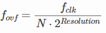
where N is the prescaler value.
2.2. CTC (Clear Timer on Compare) Mode

CTC Mode is far more precise for generating specific frequencies. Instead of waiting for an overflow at the maximum possible value, the timer counts until it matches a value you pre-defined in the Output Compare Register (OCRnx). As soon as the match occurs, the timer clears itself (resets to 0).
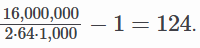
You can configure the timer to "toggle" an output pin automatically when the match occurs, creating a perfect square wave without CPU intervention. For example, to generate a 1 kHz square wave using a 16 MHz clock and a 64 prescaler, you would calculate the required OCR value:
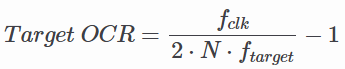
Using the values above:
2.3. PWM (Pulse Width Modulation) Mode
PWM Mode is used to simulate an analog output using digital signals. By rapidly switching a pin between HIGH and LOW, you can control the average power delivered to a component.
- Fast PWM: High frequency, suitable for power regulation and LED dimming. The timer counts from 0 to MAX, resetting to 0 immediately. The output pin changes state when the timer reaches the OCR value.
- Phase Correct PWM: Provides a symmetrical waveform by counting up to MAX and then counting back down to 0. This is preferred for motor control as it reduces electromagnetic noise. Duty Cycle: Controlled by the value in the OCR register. A higher value means the signal stays "HIGH" longer within one period.
3. Timer0
3.1. TCNT0 (Timer/Counter 0 Register)

The TCNT0 register is the core component of the 8-bit TIMER0 module. It acts as the actual counter that holds the current timer value. The value of TCNT0 increments (or decrements in certain PWM modes) based on the selected clock source and prescaler.
Users can read from or write to this register at any time. Note that manually writing a value to TCNT0 while the timer is running can cause the timer to "miss" a Compare Match with the OCR0x registers. This happens because the hardware comparison occurs in the clock cycle following a TCNT0 update.
In PWM modes, TCNT0 is constantly compared against OCR0A and OCR0B. When the values match, the output pins (OC0A/OC0B) toggle, clear, or set, depending on the configuration.
3.2. TCCR0 (Timer/Counter 0 Control Register)
In the ATmega328P, the control functionality is split into two registers: TCCR0A and TCCR0B. Together, they define the timer's behavior, including waveform generation, output modes, and clock scaling.
3.2.1. TCCR0A (Control Register A)

- Bit 7:6 - COM0A1:0 (Compare Match Output Mode A): Controls the behavior of the OC0A pin when TCNT0 matches OCR0A.
- Bit 5:4 - COM0B1:0 (Compare Match Output Mode B): Controls the behavior of the OC0B pin when TCNT0 matches OCR0B.
- Bit 1:0 - WGM01:0 (Wave Generation Mode): Combined with WGM02 in TCCR0B to select the timer mode (Normal, CTC, Fast PWM, Phase Correct PWM).
3.2.1.1. COM0x1:0 Description
This table shows the COM0x1:0 functionality when the timer is in a non-PWM mode (normal or CTC):
| COM0x1 | COM0x0 | Description |
|---|---|---|
| 0 | 0 | Normal port operation, OC0x disconnected. |
| 0 | 1 | Toggle OC0x on Compare Match. |
| 1 | 0 | Clear OC0x on Compare Match (Set output to low). |
| 1 | 1 | Set OC0x on Compare Match (Set output to high). |
3.2.1.2. WGM02:0 Description
This table shows how the WGM02:0 bits affect the counting sequence of the counter, the source for maximum (TOP) counter value, and what type of waveform generation to be used:
| WGM02 | WGM01 | WGM00 | Timer/Counter Mode of Operation | TOP | Update of OCRx at | TOV Flag Set on |
|---|---|---|---|---|---|---|
| 0 | 0 | 0 | Normal | 0xFF | Immediate | MAX |
| 0 | 0 | 1 | PWM, phase correct | 0xFF | TOP | BOTTOM |
| 0 | 1 | 0 | CTC | OCRA | Immediate | MAX |
| 0 | 1 | 1 | Fast PWM | 0xFF | BOTTOM | MAX |
| 1 | 0 | 0 | Reserved | — | — | — |
| 1 | 0 | 1 | PWM, phase correct | OCRA | TOP | BOTTOM |
| 1 | 1 | 0 | Reserved | — | — | — |
| 1 | 1 | 1 | Fast PWM | OCRA | BOTTOM | TOP |
Notes:
- MAX: 0xFF
- BOTTOM: 0x00
- Update of OCRx at: When the hardware actually updates the value of the Compare Register if you change it while the timer is running.
3.2.2. TCCR0B (Control Register B)

- Bit 7 - FOC0A (Force Output Compare A): Only active in non-PWM modes. Writing
1forces an immediate match on OC0A. - Bit 6 - FOC0B (Force Output Compare B): Only active in non-PWM modes. Writing
1forces an immediate match on OC0B. - Bit 3 - WGM02 (Waveform Generation Mode): Works with WGM01:0 to set the mode.
- Bit 2:0 - CS02:0 (Clock Select): Sets the prescaler or selects an external clock source.
3.2.2.1. CS02:0 Prescaler Settings
| CS02 | CS01 | CS00 | Description |
|---|---|---|---|
| 0 | 0 | 0 | No clock source (Timer/Counter stopped) |
| 0 | 0 | 1 | clk / 1 (No prescaling) |
| 0 | 1 | 0 | clk / 8 (From prescaler) |
| 0 | 1 | 1 | clk / 64 (From prescaler) |
| 1 | 0 | 0 | clk / 256 (From prescaler) |
| 1 | 0 | 1 | clk / 1024 (From prescaler) |
| 1 | 1 | 0 | External clock source on T0 pin. Clock on falling edge. |
| 1 | 1 | 1 | External clock source on T0 pin. Clock on rising edge. |
3.3. TIFR0 (Timer/Counter 0 Interrupt Flag Register)

- Bit 2 - OCF0B (Output Compare Flag B): Set to
1when TCNT0 matches the value in OCR0B. - Bit 1 - OCF0A (Force Output Compare A): Set to
1when TCNT0 matches the value in OCR0A. - Bit 0 - TOV0 (Timer Overflow Flag): Set to
1when the timer overflows (reaches its MAX value and restarts from 0).
4. Timer1
4.1. TCNT1 (Timer/Counter Register)

TCNT1 is functionally the same as TCNT0, serving as the core counter for its respective module, with several significant additions and architectural differences. TCNT1 is a 16-bit register divided into two 8-bit register, TCNT1H (high byte) and TCNT1L (low byte). This allows it to count from 0 to 65,535, providing much higher precision and longer timing.
TCNT1 includes a specialized Input Capture feature not found in Timer0. When a signal event occurs on the ICP1 pin, the current value of TCNT1 is instantly copied into the ICR1 register. This is used to measure external pulse widths with high accuracy.
4.2. TCCR1 (Timer/Counter 1 Control Register)
4.2.1. TCCR1A (Control Register A)

- Bit 7:6 - COM10A1:0 (Compare Match Output Mode A): Controls the behavior of the OC1A pin when TCNT1 matches OCR1A.
- Bit 5:4 - COM1B1:0 (Compare Match Output Mode B): Controls the behavior of the OC1B pin when TCNT1 matches OCR1B.
- Bit 1:0 - WGM11:0 (Wave Generation Mode): Combined with WGM13:12 in TCCR1B to select one of 16 available modes.
4.2.1.1. COM1x1:0 Description
This table shows the COM1x1:0 functionality when the timer is in a non-PWM mode (normal or CTC):
| COM1x1 | COM1x0 | Description |
|---|---|---|
| 0 | 0 | Normal port operation, OC1x disconnected. |
| 0 | 1 | Toggle OC1x on Compare Match. |
| 1 | 0 | Clear OC1x on Compare Match (Set output to low). |
| 1 | 1 | Set OC1x on Compare Match (Set output to high). |
4.2.1.2. WGM13:0 Description
This table shows how the WGM13:0 bits affect the counting sequence of the counter, the source for maximum (TOP) counter value, and what type of waveform generation to be used:
| Mode | WGM13 | WGM12 | WGM11 | WGM10 | Timer/Counter Mode of Operation | TOP | Update of OCR1x at | TOV1 Flag Set on |
|---|---|---|---|---|---|---|---|---|
| 0 | 0 | 0 | 0 | 0 | Normal | 0xFFFF | Immediate | MAX |
| 1 | 0 | 0 | 0 | 1 | PWM, phase correct, 8-bit | 0x00FF | TOP | BOTTOM |
| 2 | 0 | 0 | 1 | 0 | PWM, phase correct, 9-bit | 0x01FF | TOP | BOTTOM |
| 3 | 0 | 0 | 1 | 1 | PWM, phase correct, 10-bit | 0x03FF | TOP | BOTTOM |
| 4 | 0 | 1 | 0 | 0 | CTC | OCR1A | Immediate | MAX |
| 5 | 0 | 1 | 0 | 1 | Fast PWM, 8-bit | 0x00FF | BOTTOM | TOP |
| 6 | 0 | 1 | 1 | 0 | Fast PWM, 9-bit | 0x01FF | BOTTOM | TOP |
| 7 | 0 | 1 | 1 | 1 | Fast PWM, 10-bit | 0x03FF | BOTTOM | TOP |
| 8 | 1 | 0 | 0 | 0 | PWM, phase and frequency correct | ICR1 | BOTTOM | BOTTOM |
| 9 | 1 | 0 | 0 | 1 | PWM, phase and frequency correct | OCR1A | BOTTOM | BOTTOM |
| 10 | 1 | 0 | 1 | 0 | PWM, phase correct | ICR1 | TOP | BOTTOM |
| 11 | 1 | 0 | 1 | 1 | PWM, phase correct | OCR1A | TOP | BOTTOM |
| 12 | 1 | 1 | 0 | 0 | CTC | ICR1 | Immediate | MAX |
| 13 | 1 | 1 | 0 | 1 | (Reserved) | — | — | — |
| 14 | 1 | 1 | 1 | 0 | Fast PWM | ICR1 | BOTTOM | TOP |
| 15 | 1 | 1 | 1 | 1 | Fast PWM | OCR1A | BOTTOM | TOP |
4.2.2. TCCR1B (Control Register B)

- Bit 7 - ICNC1 (Input Capture Noise Canceler): When set to
1, a digital filter is activated on the ICP1 pin. It requires four matching cycles to trigger, reducing noise spikes. - Bit 6 - ICES1 (Input Capture Edge Select): Selects which edge triggers a capture on the ICP1 pin.
1= Rising edge;0= Falling edge. - Bit 3 - WGM13:2 (Waveform Generation Mode): Works with WGM11:0 to set the mode.
- Bit 2:0 - CS12:0 (Clock Select): Sets the prescaler or selects an external clock source.
4.2.2.1. CS02:0 Prescaler Settings
| CS12 | CS11 | CS10 | Description |
|---|---|---|---|
| 0 | 0 | 0 | No clock source (Timer/Counter stopped) |
| 0 | 0 | 1 | clk / 1 (No prescaling) |
| 0 | 1 | 0 | clk / 8 (From prescaler) |
| 0 | 1 | 1 | clk / 64 (From prescaler) |
| 1 | 0 | 0 | clk / 256 (From prescaler) |
| 1 | 0 | 1 | clk / 1024 (From prescaler) |
| 1 | 1 | 0 | External clock source on T0 pin. Clock on falling edge. |
| 1 | 1 | 1 | External clock source on T0 pin. Clock on rising edge. |
4.2.3. TCCR1C (Control Register C)

- Bit 7 - FOC1A (Force Output Compare A): Only active in non-PWM modes. Writing
1forces an immediate match on OC1A. - Bit 6 - FOC1B (Force Output Compare B): Only active in non-PWM modes. Writing
1forces an immediate match on OC1B.
4.3. TIFR1 (Timer/Counter 1 Interrupt Flag Register)

- Bit 5 - ICF1 (Input Capture Flag): Set to
1when a capture event occurs on the ICP1 pin. - Bit 2 - OCF1B (Output Compare Flag B): Set to
1when TCNT1 matches the value in OCR1B. - Bit 1 - OCF1A (Force Output Compare A): Set to
1when TCNT1 matches the value in OCR1A. - Bit 0 - TOV1 (Timer Overflow Flag): Set to
1when the timer overflows (reaches its MAX value and restarts from 0).
5. Delay Using Timers
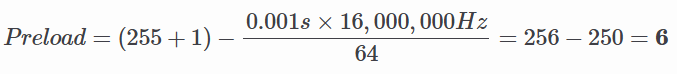
5.1. Delay Calculation in Normal Mode
In Normal Mode, the timer always counts up to its maximum value and then overflows. To get a specific delay, you preload the TCNTn register with a starting value so it only has to count a specific number of steps before overflowing.
Here is the formula to find the required preload value:
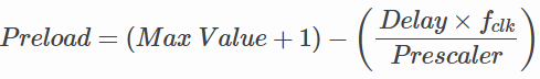
For example, if we want to create a 1ms delay using Timer0 with 1/64 presacaler:
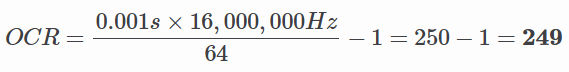
5.2. Delay Calculation in CTC Mode
In CTC (Clear Timer on Compare) Mode, the timer is much easier to use for delays because the hardware automatically resets the counter to zero when it reaches a target value stored in the OCRnx (Output Compare Register).
Here is the formula to find the value to put in OCRnx register:
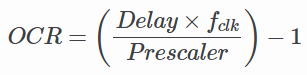
For example, if we want to create a 1ms delay using Timer0 with 1/64 presacaler:
6. Der Code
6.1. Code Example 1 (Timer0)
This code toggles PD5 every 0.5s. The delay_timer0 subroutine uses Timer0 in CTC Mode with a 1024 prescaler and a compare value of 156, creating a 10ms hardware delay per call. This subroutine is called 50 times using software loop with R18 as the counter.
;------------------------
; Assembly Code
;------------------------
#define __SFR_OFFSET 0x00
#include "avr/io.h"
;------------------------
.global main
;===============================================================
    main:
    LDI R16, 0b00100000 ; to toggle PD5
    LDI R17, 0b00000000
    ;--------------------------------------------
    SBI DDRD, 5         ; set PD5 for o/p
    OUT PORTD, R17      ; PD5 = 0
    ;--------------------------------------------
    LDI R18, 50         ; set loop counter
l1: RCALL delay_timer0  ; apply delay via timer0
    DEC R18
    BRNE l1             ; & go back & repeat
    ;--------------------------------------------
    EOR R17, R16        ; R17 = R17 XOR R16
    OUT PORTD, R17      ; toggle PD5
    LDI R18, 50         ; re-set loop counter
    RJMP l1             ; go back & repeat toggle
;===============================================================
delay_timer0:           ; ~10ms delay via Timer0
    ;---------------------------------------------------------
    CLR R20
    OUT TCNT0, R20      ; initialize timer0 with count=0
    LDI R20, 156
    OUT OCR0A, R20      ; OCR0 = 9
    LDI R20, 0b00000010
    OUT TCCR0A, R20
    LDI R20, 0b00000101
    OUT TCCR0B, R20     ; timer0: CTC mode, prescaler 1024
    ;---------------------------------------------------------
l2: IN R20, TIFR0       ; get TIFR0 byte & check
    SBRS R20, OCF0A     ; if OCF0=1, skip next instruction
    RJMP l2             ; else, loop back & check OCF0 flag
    ;---------------------------------------------------------
    CLR R20
    OUT TCCR0B, R20     ; stop timer0
    ;---------------------------------------------------------
    LDI R20, (1<<OCF0A)
    OUT TIFR0, R20      ; clear OCF0 flag
    RET
6.2. Code Example 2 (Timer1)
This code toggles PD5 every 0.5s (just like Code Example 1). The delay_timer1 subroutine uses Timer1 in Normal Mode with a 1024 prescaler and a preload value of 57724, creating a 500ms hardware delay per call.
;------------------------
; Assembly Code
;------------------------
#define __SFR_OFFSET 0x00
#include "avr/io.h"
;------------------------
.global main
;===============================================================
main:
    LDI R16, 0b00100000 ; to toggle PD5
    LDI R17, 0b00000000
    ;---------------------------------------------
    SBI DDRD, 5         ; set PD5 for o/p
    OUT PORTD, R17      ; PD5 = 0
    ;---------------------------------------------
l1: RCALL delay_timer1  ; 0.5 sec delay via timer1
    ;---------------------------------------------
    EOR R17, R16        ; R17 = R17 XOR R16
    OUT PORTD, R17      ; toggle PD5
    LDI R18, 61         ; re-set loop counter
    RJMP l1             ; go back & repeat toggle
;===============================================================
delay_timer1:           ; 0.5 sec delay via timer1
;-------------------------------------------------------
    .EQU value, 57724   ; value to give 0.5 sec delay
    LDI R20, hi8(value)
    STS TCNT1H, R20
    LDI R20, lo8(value)
    STS TCNT1L, R20     ; initialize counter TCNT1 = value
    ;-------------------------------------------------------
    LDI R20, 0b00000000
    STS TCCR1A, R20
    LDI R20, 0b00000101
    STS TCCR1B, R20     ; normal mode, prescaler = 1024
    ;-------------------------------------------------------
l2: IN R20, TIFR1       ; get TIFR1 byte & check
    SBRS R20, TOV1      ; if TOV1=1, skip next instruction
    RJMP l2             ; else, loop back & check TOV1 flag
    ;-------------------------------------------------------
    LDI R20, 1<<TOV1
    OUT TIFR1, R20      ; clear TOV1 flag
    ;-------------------------------------------------------
    LDI R20, 0b00000000
    STS TCCR1B, R20     ; stop timer1
    RET
Module 6 - Interrupt
1. Introduction to Interrupt
An interrupt is a mechanism used in microcontroller programming to pause the execution of the current program and call a specific routine or function when a particular event occurs. These events, defined by the programmer, can range from a specific condition on an input pin to a timer overflow or other hardware-defined triggers. Once the routine or function finishes executing, the program resumes from the exact point where it was interrupted.
The Arduino Uno (ATMega328P) provides two primary types of interrupts: External Interrupts and Timer Interrupts. While their functions and triggers differ, they share the same goal: interrupting the main program flow to handle specific events immediately.
External Interrupt
An External Interrupt is triggered by a change in the voltage level on specific input pins of the microcontroller. On the Arduino Uno, there are two pins dedicated to external interrupts: Pin 2 and Pin 3. These are the most commonly used pins when implementing interrupts via the Arduino programming language.
External Interrupts: INT0 and INT1
While the Arduino IDE refers to these simply as Pin 2 and Pin 3, the ATMega328P datasheet identifies them as INT0 and INT1. These are hardware-level designations that correspond to specific physical pins.
- INT0 (Digital Pin 2): This is the first external interrupt. It has a higher priority in the Interrupt Vector Table than INT1, meaning if both occur at the exact same time, the microcontroller will handle INT0 first.
- INT1 (Digital Pin 3): This is the second external interrupt.
Trigger Modes
Both INT0 and INT1 can be configured to trigger the Interrupt Service Routine (ISR) based on four specific signal states:
- LOW: Triggered whenever the pin is at a logic low level.
- CHANGE: Triggered whenever the pin changes value (High to Low or Low to High).
- RISING: Triggered specifically when the pin goes from Low to High.
- FALLING: Triggered specifically when the pin goes from High to Low.
Internal Interrupt
An Internal Interrupt is triggered by modules located inside the microcontroller itself. In the ATMega328P, these are generated by timers and are referred to as Timer Interrupts. A Timer Interrupt is specifically triggered by a timer overflow. The Arduino Uno features three internal timers: Timer0, Timer1, and Timer2. (For more details on how timers operate, please refer to the previous module).
To expand on the specific hardware components of the ATMega328P (the heart of the Arduino Uno), we need to look at how the microcontroller labels and manages these specific interrupt sources.
Internal Interrupts: Timer0, Timer1, and Timer2
The Arduino Uno has three hardware timers, each capable of generating interrupts. These are essential for tasks that require precise timing without blocking the void loop().

1. Timer0 (8-bit)
- Role: This timer is used by the Arduino internal functions like
delay(),millis(), andmicros(). - Interrupt Potential: It can trigger an Overflow Interrupt (when the counter hits 255 and resets to 0) or a Compare Match Interrupt.
- Note: Modifying Timer0 registers directly is generally discouraged because it will break the Arduino's built-in time-keeping functions.
2. Timer1 (16-bit)
- Role: Because it is a 16-bit timer, it can count up to 65,535. This allows for much longer and more precise timing intervals than Timer0 or Timer2.
- Use Case: It is frequently used by the
Servolibrary. - Interrupt Potential: Like Timer0, it supports Overflow and Compare Match interrupts, but with much higher resolution.
3. Timer2 (8-bit)
- Role: This is another 8-bit timer, similar to Timer0, but it is "independent" of the main time-keeping functions.
- Use Case: It is commonly used by the
tone()library for generating audio frequencies. - Interrupt Potential: It is an excellent choice for a custom periodic interrupt (e.g., checking a sensor every 1ms) without interfering with
delay().
2. Interrupt Handler
On the ATMega328P microcontroller, there are three essential requirements that must met to enable an interrupt:
- Global Interrupt Enabled: Interrupts must be allowed to occur globally across any part of the program. While the Arduino environment typically enables this by default, it is important to verify this when using different microcontrollers or during troubleshooting.
- Individual Interrupt Enabled: Each specific interrupt must be permitted to occur via dedicated interrupt control registers.
- Interrupt Condition Met: The microcontroller must receive a signal (either internal or external) that matches the predefined trigger criteria.
To enable a microcontroller to process interrupts, several steps must be followed. This module organizes these steps according to their placement in the code for easier implementation. The first step involves preparing the Interrupt Handler the specific code that will run when the interrupt is triggered.

Microcontrollers use a specialized memory block called the Interrupt Vector Table. This table stores the memory addresses of the programs to be executed for each specific type of interrupt.
| Vector No. | Program Address | Source | Interrupt Definition |
|---|---|---|---|
| 1 | 0x0000 | RESET | External pin, Power-on Reset, Brown-Out Reset, Watchdog System Reset |
| 2 | 0x0002 | INT0 | External Interrupt Request 0 |
| 3 | 0x0004 | INT1 | External Interrupt Request 1 |
| 4 | 0x0006 | PCINT0 | Pin Change Interrupt Request 0 |
| 5 | 0x0008 | PCINT1 | Pin Change Interrupt Request 1 |
| 6 | 0x000A | PCINT2 | Pin Change Interrupt Request 2 |
| 7 | 0x000C | WDT | Watchdog Time-out Interrupt |
| 8 | 0x000E | TIMER2_COMPA | Timer/Counter2 Compare Match A |
| 9 | 0x0010 | TIMER2_COMPB | Timer/Counter2 Compare Match B |
| 10 | 0x0012 | TIMER2_OVF | Timer/Counter2 Overflow |
| 11 | 0x0014 | TIMER1_CAPT | Timer/Counter1 Capture EVent |
| 12 | 0x0016 | TIMER1_COMPA | Timer/Counter1 Compare Match A |
| 13 | 0x0018 | TIMER1_COMPB | Timer/Counter1 Compare Match A |
| 14 | 0x001A | TIMER1_OVF | Timer/Counter1 Overflow |
| 15 | 0x001C | TIMER0_COMPA | Timer/Counter0 Compare Match A |
| 16 | 0x001E | TIMER0_COMPB | Timer/Counter0 Compare Match B |
| 17 | 0x0020 | TIMER0_OVF | Timer/Counter0 Overflow |
| 18 | 0x0022 | SPI STC | SPI Serial Transfer Complete |
| 19 | 0x0024 | USART_RX | Usart Rx Complete |
| 20 | 0x0026 | USART_UDRE | Usart Data Register Empty |
| 21 | 0x0028 | USART_TX | Usart Tx Complete |
| 22 | 0x002A | ADC | ADC Conversion Complete |
| 23 | 0x002C | EE READY | EEPROM Ready |
| 24 | 0x002E | ANALOG COMP | Analog Comparator |
These addresses are fixed and cannot be changed. When an interrupt occurs, the microcontroller automatically jumps to the corresponding address in the Interrupt Vector Table to execute the associated program.
For example if an external interrupt (INT0) is triggered, the microcontroller will jump to address 0x0002 to execute the code defined in that location.
See the program address between INT0 and INT1, which are 0x0002 and 0x0004 respectively. The gap between these addresses is only 2 bytes, which is the size of a single instruction in AVR assembly language. This means that the interrupt handler for INT0 must be concise and fit within this limited space, often requiring the use of a jump instruction to redirect to a larger block of code if necessary.
Example:
#define __SFR_OFFSET 0x00
#include "avr/io.h"

.org 0x0002	 ; external interrupt 0 vector
    rjmp toggle_led

.global main

main:
 ; your main program here

toggle_led:
    ; main interrupt logic here
    in r16, PORTB
    eor r16, (1<<PB5)
    out PORTB, r16
    reti ; return from interrupt
From the above example, we have initialized the handler for the interrupt, and then created a routine named toggle_led, which contains the code that will be executed when the interrupt is triggered. When an INT0 occurs (for example, when a button connected to the INT0 pin is pressed), the microcontroller will jump to the toggle_led routine. After performing the necessary actions, we need to inform the microcontroller that the interrupt has been successfully handled and to continue with the main program. We can use the keyword RETI, which stands for Return from Interrupt, to achieve this.
An interrupt will take priority over the main program, meaning that when an interrupt occurs, the microcontroller will temporarily halt the execution of the main program to execute the interrupt handler. Programmer must be cautious when writing interrupt handlers, as they should be efficient and not contain long-running code, to avoid delaying the main program for too long.
Using Vector Names
Instead of using raw addresses for interrupts, AVR assembly language provides predefined vector names that can be used to improve code readability. For example, instead of using .org 0x0002 for the INT0 interrupt, we can use the predefined name INT0_vect as follows:
#define __SFR_OFFSET 0x00
#include "avr/io.h"

.global INT0_vect ; declare the interrupt vector as global
.global main

main:
 ; your main program here

INT0_vect: ; Toggle LED
    in r16, PORTB
    ldi r17, (1 << 5)
    eor r16, r17 ; Toggle PB5
    out PORTB, r16
    reti
Pro tip: Just always use Vector Names instead of raw addresses :)
3. External Interrupt Registers
For detailed information about the registers, please refer to the Atmega32p datasheet. here
From the previous section, we have set up the interrupt handler for external interrupt 0. Now, we will set up the registers to setup/initialize this interrupt. Let's say we want to toggle an LED on pin PB5 with falling edge trigger. We can write the following code in our setup section:
#define __SFR_OFFSET 0x00
#include "avr/io.h"

.global main
.global INT0_vect

main:
    ; initialize external interrupt 0
    ldi r16, (1<<ISC01) ; Set ISC01 bit = 1 | trigger on falling edge
    sts EICRA, r16 ; write to EICRA register to set the interrupt trigger condition
    ldi r16, (1<<INT0) ; set INT0 bit = 1 | enable external interrupt 0
    sts EIMSK, r16 ; write to EIMSK register to enable the interrupt

    ; enable global interrupts
    sei

INT0_vect:
    ; main interrupt logic here
    in r16, PORTB
    ldi r17, (1 << 5)
    eor r16, r17 ; Toggle PB5
    out PORTB, r16
    reti
Let's break it down register by register:
EICRA (External Interrupt Control Register A)

- This register is used to configure the trigger condition for external interrupts. For INT0, we need to set the ISC01 bit to 1 and ISC00 bit to 0 for falling edge trigger. This is done by loading the value
(1<<ISC01)into register r16 and then writing it to EICRA.

EIMSK (External Interrupt Mask Register)

- This register is used to enable or disable external interrupts. To enable INT0, we need to set the INT0 bit to 1. This is done by loading the value
(1<<INT0)into register r16 and then writing it to EIMSK.
sei (Set Global Interrupt Enable)
This instruction enables global interrupts. It MUST be called after setting up the individual interrupt configurations to allow the microcontroller to respond to interrupts.
You should get the rough idea for INT1 as well. You just need to set the ISC11 and ISC10 bits in EICRA for the trigger condition and set the INT1 bit in EIMSK to enable it. Read the datasheet for more details on the trigger conditions for INT1.
4. Internal/Timer Interrupts
Internal Interrupts
Now Internal interrupts or Timer interrupts is somewhat more complex then external interrupts. Before going for implementation let's understand on what use case we can use timer interrupts:
- Replacing Delay Loops: Instead of using blocking delay loops, timer interrupts can be used to perform tasks at regular intervals without halting the main program execution.
- Real-Time Clock: Timer interrupts can be used to create a real-time clock by counting the number of timer overflows or compare matches to keep track of time.
- Event Scheduling: Timer interrupts can be used to schedule events or tasks to occur at specific intervals, allowing for multitasking in embedded applications.
For now we will try replacing delay loops with TIMER1 compare match interrupt. We will set up the timer to generate an interrupt every 5 seconds and toggle an LED in the interrupt handler.
#define __SFR_OFFSET 0
#include <avr/io.h>

.global main
.global TIMER1_COMPA_vect ; The linker looks for this specific name

main:
    ; Set PB5 as output
    sbi DDRB, 5

    ; Clear r16 to use as a zero register
    clr r16
    sts TCCR1A, r16

    ; Set prescaler to 1024 and enable CTC mode (Clear Timer on Compare)
    ; CTC mode is better for toggling so you don't have to manually reset TCNT1
    ldi r17, (1 << WGM12) | (1 << CS12) | (1 << CS10)
    sts TCCR1B, r17

    ; Reset timer count
    sts TCNT1H, r16
    sts TCNT1L, r16

    ; Set compare match value (62499 = 0xF423)
    ldi r17, 0xF4
    sts OCR1AH, r17
    ldi r17, 0x23
    sts OCR1AL, r17

    ; Enable timer compare match interrupt
    ldi r17, (1 << OCIE1A)
    sts TIMSK1, r17

    sei ; Enable global interrupts

loop:
    rjmp loop

TIMER1_COMPA_vect:
    ; toggle LED on PB5
    in r16, PORTB
    ldi r17, (1 << 5)
    eor r16, r17 ; Toggle PB5
    out PORTB, r16
    reti
TCCR1A: Timer/Counter Control Register A for Timer1
- This register is used to configure the behavior of Timer1. In this code, it is set to 0, which means normal operation mode (no PWM or special modes).
TCCR1B: Timer/Counter Control Register B for Timer1
- This register is used to set the prescaler for Timer1. In this code, it is set to (1<<CS12 | 1<<CS10), which means a prescaler of 1024 is selected. This means the timer will count at a rate of the CPU clock divided by 1024.
TCNT1L and TCNT1H: Timer/Counter Register for Timer1
- These registers hold the current count value of Timer1. They are reset to 0 at the beginning of the main function to start counting from 0. TCNTL will increment with each timer tick, and when it reaches the value set in OCR1A, it will trigger the compare match interrupt.
OCR1AL and OCR1AH: Output Compare Register for Timer1
- These registers hold the value that Timer1 will compare against. When the timer count (TCNT1) matches the value in OCR1A, the compare match interrupt will be triggered. In this code, OCR1A is set to 62499, which corresponds to a 5-second interval with a 16 MHz clock and a prescaler of 1024.
TIMSK: Timer/Counter Interrupt Mask Register
- This register is used to enable or disable specific timer interrupts. In this code, it is set to (1<<OCIE1A), which enables the Timer1 Compare Match A interrupt.
sei: Set Global Interrupt Enable
- This instruction enables global interrupts, allowing the microcontroller to respond to interrupt requests. It must be called after configuring the interrupts to ensure that the microcontroller can handle them when they occur.
TO DO: Leaern more about timer interrupts (TIMER0, TIMER2) from the official datasheet
Module 7 - PWM and EEPROM
1. PWM (Pulse Width Modulation)
PWM is a technique used to simulate analog output using a digital signal. Instead of producing a true analog voltage, the microcontroller rapidly switches a pin between HIGH and LOW.
| Term | Meaning |
|---|---|
| Period | Total time of one cycle |
| Duty Cycle | Percentage of time signal is HIGH |
Changing the duty cycle changes the average voltage seen by external devices.
AVR microcontrollers provide hardware timers that can automatically generate PWM signals in the background. It basically switches on and off on certain positions of the counter. To generate more finely controlled PWM output (such as those for servos), Timer1 is usually used as it is 16 bits thus allowing more precise features.
Phase Correct PWM
Phase correct PWM uses dual slop that goes up and down, switching between those operations. This mode performs more accurately in exchange for half the available frequency.
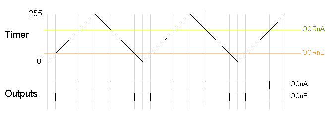
Fast PWM
Fast PWM provides PWM with higher frequency but lower resolution because it uses a single-slope operation, where the counter immediately returns to 0 after reaching its maximum value. Fast PWM is commonly used for devices that require high-frequency signals.
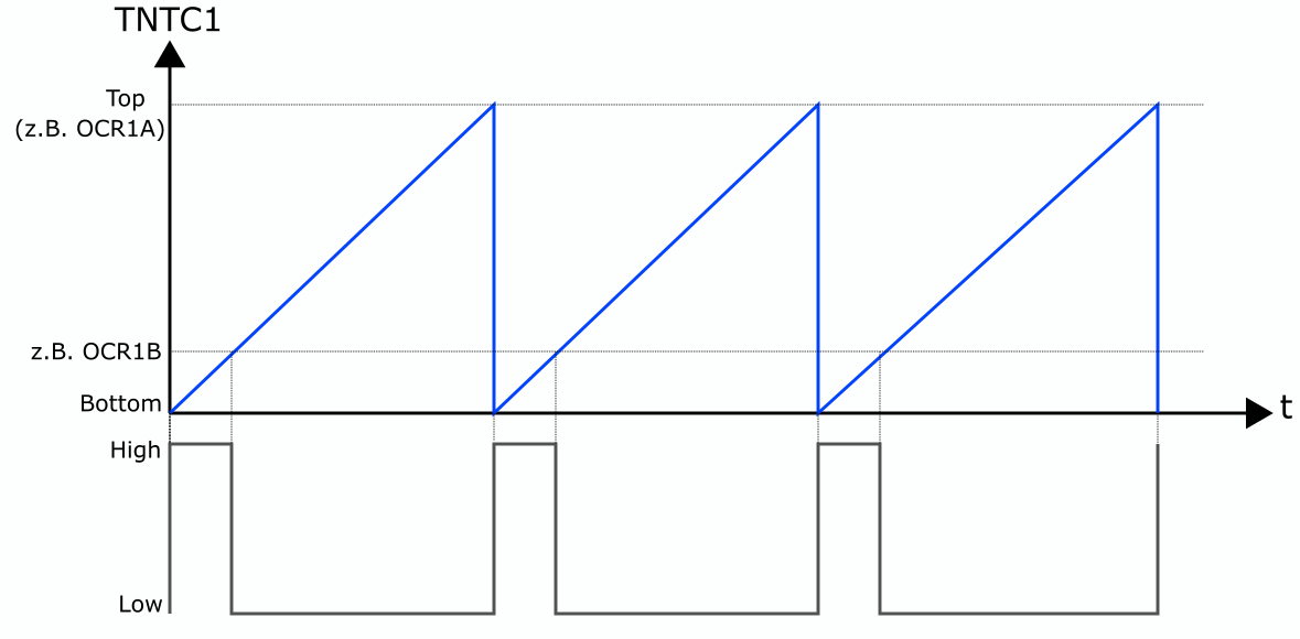
TCCRnA and TCCRnB — Timer/Counter Control Registers
TCR1A
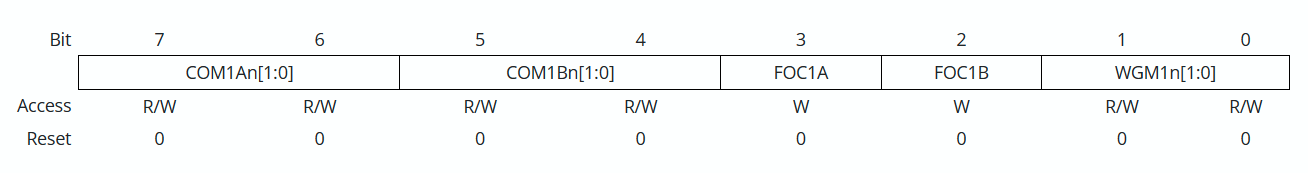
TCR1B
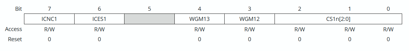
COM
| COM1x1 | COM1x0 | Description |
|---|---|---|
| 0 | 0 | Normal port operation (PWM disconnected) |
| 0 | 1 | Toggle OC1X on Compare Match (special case) |
| 1 | 0 | Clear on Compare Match, Set at BOTTOM (Non-inverting PWM) |
| 1 | 1 | Set on Compare Match, Clear at BOTTOM (Inverting PWM) |
WGM
Certain modes in the Timer that affects PWM behavior
| Mode | WGM13 | WGM12 | WGM11 | WGM10 | Mode Name | TOP |
|---|---|---|---|---|---|---|
| 1 | 0 | 0 | 0 | 1 | PWM Phase Correct 8-bit | 0x00FF |
| 2 | 0 | 0 | 1 | 0 | PWM Phase Correct 9-bit | 0x01FF |
| 3 | 0 | 0 | 1 | 1 | PWM Phase Correct 10-bit | 0x03FF |
| 5 | 0 | 1 | 0 | 1 | Fast PWM 8-bit | 0x00FF |
| 6 | 0 | 1 | 1 | 0 | Fast PWM 9-bit | 0x01FF |
| 7 | 0 | 1 | 1 | 1 | Fast PWM 10-bit | 0x03FF |
| 8 | 1 | 0 | 0 | 0 | PWM Phase & Frequency Correct (ICR1) | ICR1 |
| 9 | 1 | 0 | 0 | 1 | PWM Phase & Frequency Correct (OCR1A) | OCR1A |
| 10 | 1 | 0 | 1 | 0 | PWM Phase Correct (ICR1) | ICR1 |
| 11 | 1 | 0 | 1 | 1 | PWM Phase Correct (OCR1A) | OCR1A |
| 14 | 1 | 1 | 1 | 0 | Fast PWM (ICR1 TOP) | ICR1 |
| 15 | 1 | 1 | 1 | 1 | Fast PWM (OCR1A TOP) | OCR1A |
OCRn — Output Compare Register
The Output Compare Register stores a value that the timer constantly compares against the counter. When the counter hits that value, it triggers compare match that does different things aaccording to COM to the set output pin.
- Setting a pin HIGH
- Clearing a pin LOW
- Triggering an interrupt
ICRn — Input Capture Register
The Input Capture Register is used in certain PWM modes as the TOP value of the timer. This means the timer counts from 0 up to the value stored in ICRn before restarting the counting cycle.
When used as TOP, ICRn determines the PWM period (frequency).
In PWM modes that use ICRn as TOP (such as mode 8 & 15), the timer behavior becomes:
Counter: 0 → ICRn → reset
Changing ICRn changes the PWM frequency, while OCRn still controls the duty cycle.
2. Servos
Servos are motors that adjusts to certain angles following certain PWM pulses.
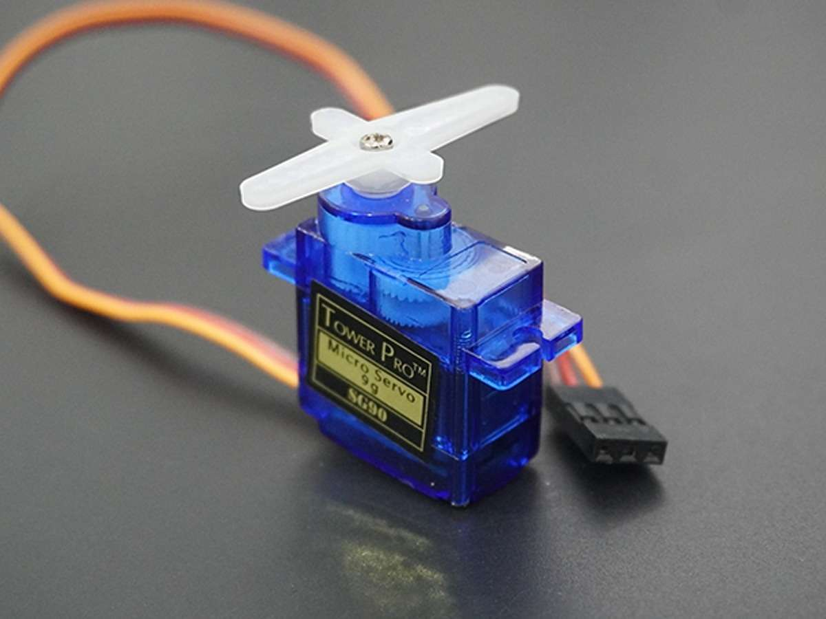
Servo Signal Operation
Servo operates with 20 ms PWM periods.
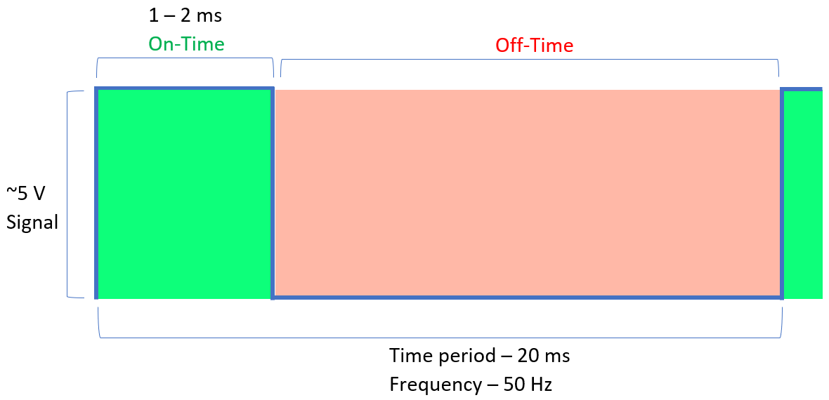
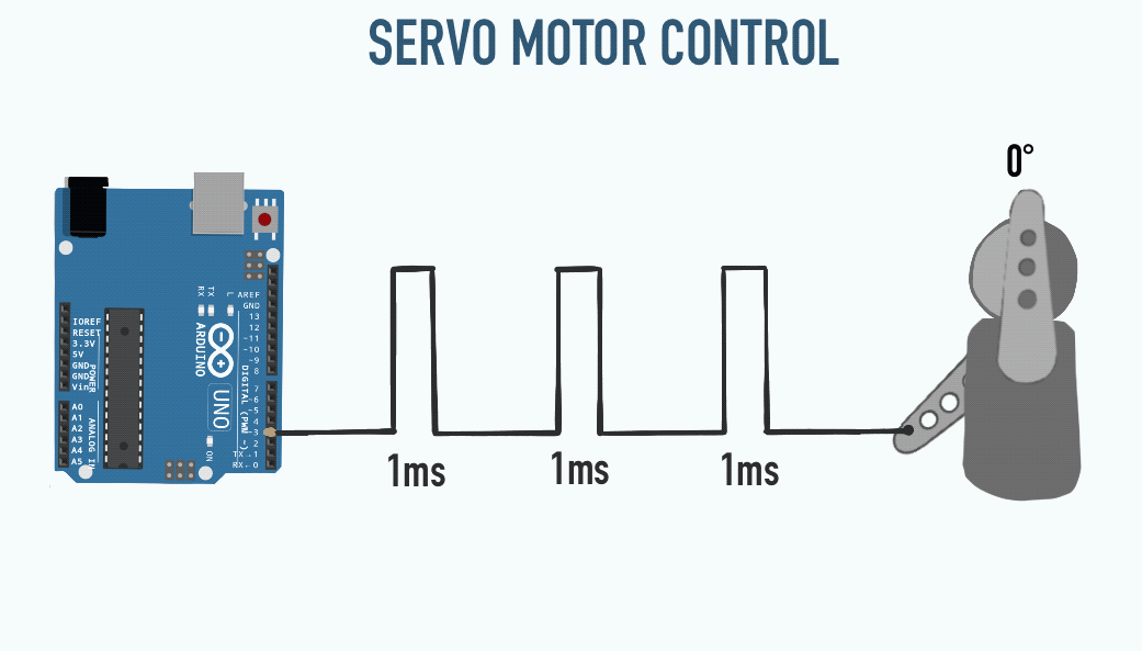
| Parameter | Typical Value |
|---|---|
| PWM Period | ≈ 20 ms |
| Pulse Width | ≈ 1 – 2 ms |
Servo operates with 20 ms PWM periods. This can hardly be achieved with Timer0 since Timer0 is an 8-bit timer.
This means its maximum counter value is:
2^8 - 1 = 255
20 ms period is hardly achievable with this which requires a 16-bit timer is preferred.
This allows precise generation of long PWM periods.
Using a prescaler of 8:
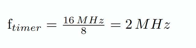
Timer tick duration:

Required servo period: 20 ms
Number of timer counts required:

Servo Initialization Code Example
SBI DDRB, 1
Configure OC1A pin as output. Timer1 will control this pin automatically.
LDI R22, (1<<COM1A1) | (1<<WGM11)
STS TCCR1A, R22
TCCR1A configuration:
| Bit | Purpose |
|---|---|
| COM1A1 = 1 | Enable PWM output on OC1A |
| WGM11 = 1 | Part of Fast PWM mode selection |
This connects Timer1 to the output pin.
LDI R22, hi8(40000)
STS ICR1H, R22
LDI R22, lo8(40000)
STS ICR1L, R22
Set ICR1 = 40000.
This is to make the Timer 1 count to 40 000 following the previous calculations.
LDI R22, (1<<WGM13) | (1<<WGM12) | (1<<CS11)
STS TCCR1B, R22
TCCR1B configuration:
| Bit | Purpose |
|---|---|
| WGM13 + WGM12 | Complete Fast PWM Mode 14 |
| CS11 = 1 | Prescaler = 8 |
This starts Timer1 in Fast PWM mode.
Servo Initialization
; Sets Timer1 PWM in PB1 to use period of 20ms by using Fast PWM.
; Timer1 counts until ICR1
SERVO_init:
  SBI DDRB, 1

  LDI R22, (1<<COM1A1) | (1<<WGM11)
  STS TCCR1A, R22

  LDI R22, hi8(40000)
  STS ICR1H, R22
  LDI R22, lo8(40000)
  STS ICR1L, R22

  LDI R22, (1<<WGM13) | (1<<WGM12) | (1<<CS11)
  STS TCCR1B, R22

  RET
Servo Usage
  .EQU LEFT, 2400  ; Generates a 2400/40000 % duty cycle.

  LDI R16, hi8(LEFT)
  STS OCR1AH, R16
  LDI R16, lo8(LEFT)
  STS OCR1AL, R16
This code makes the PWM generate compare match at count 2400 this allows it to produce a 2400/40000 * 20 ms = ~1.2 ms pulse which is around 0 degrees.
3. EEPROM
EEPROM is a small non-volatile memory inside the microcontroller.
Unlike SRAM:
- SRAM loses data when power is removed
- EEPROM keeps data even after reset or power loss
EEPROM is commonly used to store:
- Settings
- Calibration values
- System state
EEPROM has limited write endurance, so it should only be used sparingly
EEPROM Registers
EEPROM operations are controlled using dedicated I/O registers.
EEARH:EEARL — EEPROM Address Register
Stores the memory address to be accessed.
EEDR — EEPROM Data Register
Stores the data to be written or read.
EECR — EEPROM Control Register
Controls read and write operations.
Important control bits:
| Name | Bit | Function |
|---|---|---|
| EERE | 0 | EEPROM Read Enable |
| EEWE | 1 | EEPROM Write Enable |
| EEMWE | 2 | EEPROM Host Write Enable |
EEPROM Write Operation
Writing EEPROM requires a specific sequence:
- Wait until EEWE becomes ‘0’.
- Write new EEPROM address to EEAR (optional).
- Write new EEPROM data to EEDR (optional).
- Write a logical ‘1’ to the EEMWE bit while writing a ‘0’ to EEWE in EECR.
- Within four clock cycles after setting EEMWE, write a logical ‘1’ to EEWE.
; Writes R21 to EEPROM address in 0x0052
EEPROM_write:
  SBIC  EECR, 1
  RJMP  EEPROM_write

  LDI R22, hi8(0x0052)
  OUT   EEARH, R22
  LDI R22, lo8(0x0052)
  OUT   EEARL, R22

  OUT   EEDR, R21

  SBI   EECR, 2
  SBI   EECR, 1
  RET
EEPROM Read Operation
Reading EEPROM is simpler:
- Load address into EEAR
- Start read operation by setting EERE
- Read data from EEDR
; Read R21 from EEPROM address in 0x0052
EEPROM_read:
  SBIC  EECR, 1
  RJMP  EEPROM_read

  LDI R22, hi8(0x0052)
  OUT   EEARH, R22
  LDI R22, lo8(0x0052)
  OUT   EEARL, R22

  SBI   EECR, 0
  IN    R21, EEDR
  RET
4. References
PWM Basics
Servo Basics
EEPROM
Modul 8: ADC (Analog to Digital Conversion)
Amba to Digital
1. Analog vs Digital Signal
1.1 Analog Signals
Analog signals are signals that are continuous — meaning their values can change smoothly without jumps, representing physical quantities from the real world such as temperature, light, sound, and pressure.
Characteristics of analog signals:
- Values can be any real value within a range.
- Sensitive to noise (electromagnetic interference, heat, etc.).
- Interact directly with the real world (sensors, microphones, photodiodes).

1.2 Digital Signals
Digital signals are signals that are discrete — their values can only be in two conditions: HIGH (1) or LOW (0), usually in the form of a square wave.
Characteristics of digital signals:
- Only have two values: 0 and 1 (LOW and HIGH).
- Nearly immune to noise.
- Used in data transmission and processing within electronic devices.
- Use less energy.

1.3 Comparison of Analog and Digital
| Aspect | Analog Signal | Digital Signal |
|---|---|---|
| Nature | Continuous | Discrete |
| Values | All real values | 0 or 1 |
| Noise Resistance | Low | Very high |
| Primary Use | Sensors, real-world actuators | Data processing, computing |
| Examples | Microphone sound, LDR output, sensor temperature | Serial data, clock signals, PWM |
| Energy Consumption | Relatively larger | More efficient |
Both complement each other: analog signals capture real-world phenomena accurately, then are converted to digital so they can be processed by computers/microcontrollers.
2. Analog to Digital Converter (ADC)
2.1 Understanding ADC
ADC (Analog to Digital Converter) is a component or circuit that converts analog signals (continuous values) into a digital representation (discrete values in the form of binary numbers) so they can be processed by digital systems such as microcontrollers or computers.

2.2 Stages of the ADC Conversion Process
In general, the ADC process is divided into four main stages:
| No | Stage | Explanation |
|---|---|---|
| 1 | Sampling | Capturing (sampling) values from an analog signal at specific discrete points in time. The higher the sampling frequency, the more accurate the digital representation. |
| 2 | Filtering | Cleaning the signal from noise before conversion to ensure the conversion results are more accurate. NOTE: This is usually not discussed much in ADC methods |
| 3 | Quantizing | Converting the analog value at a single discrete point in time into a specific level representation. The number of levels is determined by the ADC resolution (e.g., 10-bit = 1024 levels). |
| 4 | Encoding | Converting the level value from quantization into digital binary code per discrete time unit. |
We won't go deep into this process, as you will study it directly in the Telecommunications lab next semester 😂
2.3 Illustration of the ADC Process

3. Why is ADC Needed in Embedded Systems?

The real world is analog — all physical phenomena (temperature, light, sound, pressure, humidity) are continuous signals. However, microcontrollers and computers can only process information in digital form (0 and 1).
ADC acts as a bridge between the physical world and the digital world:
- Sensors produce analog signals → For example, an LDR produces a voltage that changes according to light intensity.
- Microcontrollers only understand digital numbers → Without an ADC, a microcontroller cannot "read" that voltage value.
- ADC converts → An analog voltage of 0–5V is converted into a number from 0–1023 (for a 10-bit ADC).
- Programs can process the result → For example: if the ADC value is < 500, turn on the LED.
Examples of ADC usage in daily life:
- Reading temperature sensor values (LM35) → conversion to degrees Celsius
- Reading light intensity (LDR) → automatic screen brightness control
- Reading a potentiometer → audio volume control
- Voice recording (microphone) → audio digitization
- Battery measurement → displaying power percentage
4. ADC In ATmega328p
4.1 ATmega328p ADC Specifications
The ATmega328p (used in the Arduino Uno) has a built-in ADC with the following specifications:
| Specification | Value |
|---|---|
| Resolution | 10-bit (produces values from 0 – 1023) |
| Conversion Method | Successive Approximation |
| Input Channels | 8 analog channels (A0 – A7), multiplexed |
| Reference Voltage | AVcc, Internal 2.56V, or external AREF pin |
| Conversion Speed | 50 kHz – 200 kHz (depending on prescaler) |
| Result Registers | ADCL (low-byte) + ADCH (high-byte) |
4.2 Successive Approximation Method

The ATmega328p uses the Successive Approximation Register (SAR) method. In this method, the ADC works by performing a binary search for the Vin value.
At each step:
- The SAR sets a trial bit
- The DAC generates a voltage (Vdac)
- A comparator compares Vin with Vdac
- The bit is either kept or changed based on the comparison result
This process is repeated N times (N = ADC resolution, which is 10-bit for the ATmega328p).
An example of SAR implementation can be seen in this image:

- Started from the middle value (1000) This is the representation of ½ of Vref (MSB = 1).
- First comparison (Comparator)
- If Vdac > Vin → move down (red arrow)
- If Vdac < Vin → move up (green arrow)
- Determining the next bit
Each step determines one additional bit.
Example:
1000 → 1100(if Vin is larger)1000 → 0100(if Vin is smaller)
- Repeat process (Binary Search) The value range is continuously narrowed until all bits (MSB → LSB) are determined.
- Final result
The rightmost nodes show the final binary code.
Example results:
1011,0110, etc.
5. Important ADC Parameters In ATmega328p
5.1 Reference Voltage (Vref)
Reference Voltage (Vref) is the maximum voltage that serves as the full-scale reference in the ADC conversion process. Vref determines the range of input voltage that can be read by the ADC.
On the ATmega328p, there are three options for the reference voltage source:
| REFS1 | REFS0 | Vref Source | Description |
|---|---|---|---|
| 0 | 0 | AREF pin | Uses an external voltage connected to the AREF pin |
| 0 | 1 | AVcc | Uses the supply voltage (VCC), typically 5V |
| 1 | 0 | (unused) | — |
| 1 | 1 | Internal 2.56V | Uses a fixed internal 2.56V reference voltage, ignoring VCC |

Influence of Vref on effective resolution:
| Vref | Resolution per step |
|---|---|
| 5V (AVcc) | 5V / 1024 ≈ 4.88 mV per step |
| 2.56V (Internal) | 2.56V / 1024 ≈ 2.5 mV per step |
The smaller the Vref, the finer the resolution — but the measurable input range is also smaller.
5.2 Prescaler
The Prescaler is a frequency divider that determines the ADC clock speed from the main system clock (F_CPU). The ADC requires a clock within the range of 50 kHz – 200 kHz for accurate results.
On the ATmega328p (F_CPU = 16 MHz), prescaler options are configured via the ADPS2:ADPS0 bits in the ADCSRA register:
| ADPS2 | ADPS1 | ADPS0 | Divider | ADC Clock (at 16 MHz) |
|---|---|---|---|---|
| 0 | 0 | 0 | CLK/2 | 8 MHz |
| 0 | 0 | 1 | CLK/2 | 8 MHz |
| 0 | 1 | 0 | CLK/4 | 4 MHz |
| 0 | 1 | 1 | CLK/8 | 2 MHz |
| 1 | 0 | 0 | CLK/16 | 1 MHz |
| 1 | 0 | 1 | CLK/32 | 500 kHz |
| 1 | 1 | 0 | CLK/64 | 250 kHz |
| 1 | 1 | 1 | CLK/128 | 125 kHz ✅ (most accurate) |
Note: The recommended ADC clock is between 50 kHz–200 kHz. A CLK/128 prescaler at 16 MHz produces 125 kHz — well within the optimal range.
5.3 Conversion Rate
Conversion Rate is the number of ADC conversions that can be performed per second. Its value depends on the ADC clock and the number of clock cycles per conversion.
On the ATmega328p:
- One ADC conversion requires 13 ADC clock cycles (except for the first conversion after enabling = 25 cycles).
- Conversion Rate = ADC Clock / 13
| Prescaler | ADC Clock | Conversion Rate |
|---|---|---|
| CLK/64 | 250 kHz | ≈ 19.2 kSPS |
| CLK/128 | 125 kHz | ≈ 9.6 kSPS |
kSPS = kilo Samples Per Second (thousands of samples per second)
5.4 Influence of Vref, Prescaler, and Conversion Rate on Accuracy
These three parameters are interrelated in determining the quality of ADC conversion results, in terms of resolution, accuracy, and the ability to track signal changes.
| Parameter | Smaller Value | Larger Value |
|---|---|---|
| Vref | Finer resolution (small LSB), but limited input range | Wider input range, but coarser resolution (large LSB) |
| Prescaler (divider) | Higher ADC frequency → risk of inaccuracy if exceeding specification limits | Lower ADC frequency → more stable operation if within optimal range (50–200 kHz) |
| Conversion Rate | Sparse sampling → risk of losing information (aliasing) | More frequent sampling → better ability to track signal changes |
Conclusion:
- Vref determines the trade-off between resolution and measurement range.
- The Prescaler must be chosen so that the ADC frequency stays within the optimal range to maintain accuracy.
- The Conversion rate must be high enough (≥ 2× signal frequency, according to the Nyquist Theorem which you will learn in the 5th-semester Telecommunications lab) for the signal to be well-represented.
6. Specific Registers for ADC In ATmega328p
6.1 ADMUX — ADC Multiplexer Selection Register
ADMUX is an 8-bit register that handles the basic ADC configuration: reference voltage source, data storage format, and which analog input channel to read.

Functions of each field:
a) REFS1:REFS0 — Reference Selection
Selects the ADC reference voltage source:
| REFS1 | REFS0 | Reference Voltage |
|---|---|---|
| 0 | 0 | AREF Pin (external) |
| 0 | 1 | AVcc (supply voltage, typically 5V) |
| 1 | 0 | Unused |
| 1 | 1 | Internal 2.56V |
b) ADLAR — ADC Left Adjust Result
Determines the storage position of the 10-bit result within the two 8-bit registers (ADCH + ADCL):
| ADLAR | ADCH (8-bit) | ADCL (8-bit) |
|---|---|---|
| 1 (Left-justified) | D9 D8 D7 D6 D5 D4 D3 D2 | D1 D0 (unused 6-bit) |
| 0 (Right-justified) | (unused 6-bit) D9 D8 | D7 D6 D5 D4 D3 D2 D1 D0 |
- Right-justified (ADLAR=0): ADCL stores the bottom 8 bits, and ADCH stores the top 2 bits. Typically used for reading the full 10-bit value.
- Left-justified (ADLAR=1): ADCH stores the top 8 bits of the result. Useful when only 8-bit precision is needed (just read ADCH).
c) MUX3:MUX0 — Analog Channel Selection
Selects which analog input pin will be converted:
| MUX3 | MUX2 | MUX1 | MUX0 | Analog Pin |
|---|---|---|---|---|
| 0 | 0 | 0 | 0 | ADC0 / A0 |
| 0 | 0 | 0 | 1 | ADC1 / A1 |
| 0 | 0 | 1 | 0 | ADC2 / A2 |
| 0 | 0 | 1 | 1 | ADC3 / A3 |
| 0 | 1 | 0 | 0 | ADC4 / A4 |
| 0 | 1 | 0 | 1 | ADC5 / A5 |
| 0 | 1 | 1 | 0 | ADC6 / A6 |
| 0 | 1 | 1 | 1 | ADC7 / A7 |
6.2 ADCSRA — ADC Control and Status Register A
ADCSRA is an 8-bit register that serves as the command center for controlling and monitoring the ADC process status.

Functions of each bit:
| Bit | Name | Function |
|---|---|---|
ADEN  |
ADC Enable | Set to 1 to enable the ADC. If 0, the ADC will not run and analog pins won't be converted. |
| ADSC | ADC Start Conversion | Set to 1 to start a single conversion cycle. This bit stays at 1 while conversion is in progress, then automatically returns to 0. |
| ADATE | ADC Auto Trigger Enable | If 1, conversion starts automatically triggered by a specific event (e.g., timer overflow, external pin change). |
| ADIF | ADC Interrupt Flag | Set to 1 by hardware when conversion is complete (End of Conversion). Reset by manually writing a 1 to this bit. |
| ADIE | ADC Interrupt Enable | If 1, the program will jump to an ISR (Interrupt Service Routine) when conversion is complete. Useful so the CPU doesn't have to wait (polling). |
| ADPS2:ADPS0 | ADC Prescaler Select | 3 bits that determine the clock divider for the ADC (see the prescaler table above). |
6.3 ADCL and ADCH — ADC Data Registers
ADCL and ADCH are two 8-bit registers where the 10-bit ADC conversion result is stored after conversion is complete.
Since the ATmega328p uses a 10-bit ADC, the result (0–1023) cannot fit into a single 8-bit register, so it's split across two registers:

IMPORTANT: ADCL must be read first before ADCH. Reading ADCL locks ADCH to prevent it from changing until ADCH is read, ensuring data consistency.
How to read the full 10-bit ADC value (right-justified):
// In C:
uint16_t adc_value = ADC;  // or:
uint8_t  low  = ADCL;
uint8_t  high = ADCH;
uint16_t adc_value = (high << 8) | low;
; In Assembly:
LDS R18, ADCL    ; read low-byte first
LDS R19, ADCH    ; then read high-byte
7. ADC Conversion Flowchart
Here is the complete workflow for using the ADC on the ATmega328p:

The flowchart above illustrates the ADC reading process on the ATmega328p in single conversion mode using the polling method, with the following configuration:
-
Conversion Mode: The ADC operates in single conversion mode, meaning each conversion starts manually by setting the ADSC = 1 bit.
-
Synchronization Method: The conversion completion status is checked using polling of the ADIF bit in the ADCSRA register, instead of using interrupts.
-
Auto Trigger: This flowchart assumes ADATE = 0, so conversions do not run automatically and must be restarted by the program each time a reading is taken.
-
ADC Interrupt: This flowchart does not use ADC interrupts, so ADIE = 0.
-
Input Channel: The configuration example in the flowchart uses ADC0 (pin A0 / PC0) as the analog input channel.
-
Reference Voltage: This flowchart follows an assembly program example that uses the internal reference voltage via the configuration of the REFS1:REFS0 bits in the ADMUX register.
-
Conversion Data Format: The ADC result is stored in right-justified format (ADLAR = 0), so the full 10-bit value is read through two registers:
- ADCL as the low-byte
- ADCH as the high-byte
-
Data Register Reading Order: The ADCL register must be read first, followed by ADCH, to ensure the conversion data remains consistent.
-
ADC Prescaler: This example uses a CLK/128 prescaler (ADPS2:ADPS0 = 111). If the system clock is 16 MHz, the ADC clock becomes:

This value is within the recommended ADC operating range.
Summary of Configuration Used
- ADC Mode: Single Conversion
- Trigger Mode: Manual (
ADSC = 1) - Polling / Interrupt: Polling (
ADIF) - Auto Trigger: Disabled (
ADATE = 0) - Interrupt ADC: Disabled (
ADIE = 0) - Channel: ADC0 / A0 / PC0
- Data Alignment: Right-justified (
ADLAR = 0) - Prescaler: CLK/128
- ADC Clock: 125 kHz (if
F_CPU = 16 MHz)
8. ADC Assembly Code Example
8.1 Full Code
Here is an example of AVR Assembly code to read the ADC from the ADC0 pin using the internal 2.56V reference and a CLK/128 prescaler:
#define __SFR_OFFSET 0x00
#include "avr/io.h"
;------------------------
.global main

main:
    LDI R20, 0xFF
    OUT DDRD, R20       ; Set Port D as output (ADC result low byte)
    OUT DDRB, R20       ; Set Port B as output (ADC result high byte)
    SBI DDRC, 0         ; Set pin PC0 as input for ADC0

    ;-- ADC Initialization --
    LDI R20, 0xC0       ; REFS1:REFS0 = 11 → Internal 2.56V
                        ; ADLAR = 0 → Right-justified
                        ; MUX4:MUX0 = 00000 → ADC0
    STS ADMUX, R20

    LDI R20, 0x87       ; ADEN = 1 → Enable ADC
                        ; ADPS2:ADPS0 = 111 → Prescaler CLK/128
    STS ADCSRA, R20

;-- ADC Reading Loop --
read_ADC:
    LDI R20, 0xC7       ; Set ADSC = 1 to start conversion
    STS ADCSRA, R20

wait_ADC:
    LDS R21, ADCSRA     ; Read ADCSRA status register
    SBRS R21, 4         ; Skip jump if ADIF (bit 4) = 1 (conversion complete)
    RJMP wait_ADC       ; Wait loop until ADIF is set

    ;-- Reset ADIF flag --
    LDI R17, 0xD7       ; Set ADIF = 1 so the controller can reset the flag
    STS ADCSRA, R17

    ;-- Read conversion result --
    LDS R18, ADCL       ; Read low-byte from ADCL (MUST read first)
    LDS R19, ADCH       ; Read high-byte from ADCH

    ;-- Output result --
    OUT PORTD, R18      ; Send low-byte to Port D
    OUT PORTB, R19      ; Send high-byte to Port B

    RJMP read_ADC       ; Repeat reading
8.2 Code Explanation
Initialization Section:
LDI R20, 0xC0
STS ADMUX, R20
0xC0in binary =1100 0000- REFS1=1, REFS0=1 → Internal 2.56V reference voltage
- ADLAR=0 → Right-justified output
- MUX4:MUX0 = 00000 → Reading pin ADC0 (A0)
- This part runs only once during initialization.
LDI R20, 0x87
STS ADCSRA, R20
0x87in binary =1000 0111- ADEN=1 → ADC is enabled
- ADPS2:ADPS0 = 111 → Prescaler CLK/128 (125 kHz at 16 MHz)
Reading Section (Loop):
LDI R20, 0xC7
STS ADCSRA, R20
0xC7in binary =1100 0111- ADEN=1, ADSC=1 → Start one conversion cycle
- ADPS remains the same (CLK/128)
wait_ADC:
    LDS R21, ADCSRA
    SBRS R21, 4
    RJMP wait_ADC
- Polling loop: continuously reads ADCSRA and checks bit 4 (ADIF)
SBRS= Skip if Bit in Register Set → if ADIF=1 (conversion complete), skip RJMP- As long as ADIF=0 (conversion not complete), continue looping
LDI R17, 0xD7
STS ADCSRA, R17
- Resets the ADIF flag by writing a 1 to the ADIF bit
- This is necessary so the next conversion can be detected
LDS R18, ADCL
LDS R19, ADCH
OUT PORTD, R18
OUT PORTB, R19
- Read ADCL first (mandatory), then ADCH
- Send the results to Port D (low-byte) and Port B (high-byte)
- Since it is right-justified: ADCH only contains 2 bits (bits 9 and 8)
Module 9 - SPI, I2C, and Sensor Interfacing
1. Serial Peripheral Interface (SPI)
1.1 Overview
SPI is a synchronous serial communication protocol commonly used for fast peripheral communication in embedded systems. It typically uses four lines:
- SCK: Serial Clock
- MOSI: Master Out Slave In
- MISO: Master In Slave Out
- SS/CS: Slave Select / Chip Select
SPI is full-duplex, meaning data can be transmitted and received at the same time.
1.2 Communication Flow
- The master pulls SS low to select a slave.
- The master generates clock pulses on SCK.
- Data shifts out on MOSI and shifts in on MISO.
- The transfer ends when the expected bits/bytes are completed.
- The master releases SS high.
1.3 SPI Clock Modes
- Mode 0: CPOL = 0, CPHA = 0
- Mode 1: CPOL = 0, CPHA = 1
- Mode 2: CPOL = 1, CPHA = 0
- Mode 3: CPOL = 1, CPHA = 1
1.4 SPI Registers (Detailed Bits)
SPDR - SPI Data Register
Function:
- Stores data to transmit and received data.
| Bit | Name | Description |
|---|---|---|
| 7 | SPD7 | Data bit 7 |
| 6 | SPD6 | Data bit 6 |
| 5 | SPD5 | Data bit 5 |
| 4 | SPD4 | Data bit 4 |
| 3 | SPD3 | Data bit 3 |
| 2 | SPD2 | Data bit 2 |
| 1 | SPD1 | Data bit 1 |
| 0 | SPD0 | Data bit 0 |
SPSR - SPI Status Register
Function:
- Indicates transfer completion and collision state.
| Bit | Name | Description |
|---|---|---|
| 7 | SPIF | SPI interrupt/transfer complete flag |
| 6 | WCOL | Write collision flag |
| 5 | Reserved | Reserved |
| 4 | Reserved | Reserved |
| 3 | Reserved | Reserved |
| 2 | Reserved | Reserved |
| 1 | Reserved | Reserved |
| 0 | SPI2X | Double SPI speed (master mode) |
SPCR - SPI Control Register
Function:
- Controls SPI enable state, mode, clock settings, and interrupts.
| Bit | Name | Description |
|---|---|---|
| 7 | SPIE | Enable SPI interrupt |
| 6 | SPE | Enable SPI peripheral |
| 5 | DORD | Data order (1=LSB first, 0=MSB first) |
| 4 | MSTR | Master select (1=master, 0=slave) |
| 3 | CPOL | Clock polarity |
| 2 | CPHA | Clock phase |
| 1 | SPR1 | Clock rate select bit 1 |
| 0 | SPR0 | Clock rate select bit 0 |
Clock-rate note:
- SPI clock rate in master mode is determined by SPR1, SPR0, and SPI2X.
1.5 SPI Assembly Examples
SPI Master
;------------------------
; Assembly Code SPI Master
;------------------------
#define __SFR_OFFSET 0x00
#include "avr/io.h"
;------------------------
.global main
;==============================================================
main:
.equ  SCK, 5
.equ  MOSI, 3
.equ  SS, 2
;--------------------------------------------------------------
      LDI   R17, (1<<MOSI)|(1<<SCK)|(1<<SS)
      OUT   DDRB, R17       ;set MOSI, SCK, SS as o/p
      ;--------------------------------------------------------
      LDI   R17, (1<<SPE)|(1<<MSTR)|(1<<SPR0)
      OUT   SPCR, R17       ;enable SPI as master, fsck=fosc/16
      ;--------------------------------------------------------
      LDI   R17, 0xAA       ;byte to be transmitted
      ;--------------------------------------------------------
again:CBI   PORTB, SS       ;enable slave device
      OUT   SPDR, R17       ;transmit byte to slave
      ;--------------------------------------------------------
loop: IN    R18, SPSR
      SBRS  R18, SPIF       ;wait for byte transmission
      RJMP  loop            ;to complete
      ;--------------------------------------------------------
      SBI   PORTB, SS       ;disable slave device
      ;--------------------------------------------------------
      RCALL my_delay        ;delay
      COM   R17             ;1's compliment of byte
      RJMP  again           ;repeat transmission
;==============================================================
my_delay:                   ;delay in ms
    LDI   R20, 255
l6: LDI   R21, 255
l7: LDI   R22, 40
l8: DEC   R22
    BRNE  l8
    DEC   R21
    BRNE  l7
    DEC   R20
    BRNE  l6
    RET
SPI Slave
;------------------------
; Assembly Code SPI Slave
;------------------------
#define __SFR_OFFSET 0x00
#include "avr/io.h"
;------------------------
.global main
;============================================================
main:
;------------------------------------------------------------
      LDI   R17, 0xFF
      OUT   DDRD, R17       ;set PORTD for o/p
      ;------------------------------------------------------
      LDI   R17, (1<<SPE)
      OUT   SPCR, R17       ;enable SPI as slave
      ;------------------------------------------------------
agn:  IN    R18, SPSR
      SBRS  R18, SPIF       ;wait for byte reception
      RJMP  agn
      ;------------------------------------------------------
      IN    R18, SPDR       ;i/p byte from data register
      OUT   PORTD, R18      ;and o/p to PORTD
      ;------------------------------------------------------
      RJMP  agn             ;repeat reception
2. Inter-Integrated Circuit (I2C)
2.1 Overview
I2C is a synchronous two-wire serial bus:
- SDA: Serial Data
- SCL: Serial Clock
I2C supports multiple devices on the same bus using slave addressing and ACK/NACK handshaking.
2.2 I2C Transaction Flow
- Master sends START condition.
- Master sends Slave Address + R/W bit.
- Slave replies with ACK.
- Data bytes are exchanged with ACK/NACK after each byte.
- Master sends STOP condition.
2.3 I2C Speed Modes
- Standard mode: up to 100 kHz
- Fast mode: up to 400 kHz
- Fast mode plus: up to 1 MHz
- High-speed mode: up to 3.4 MHz
- Ultra-fast mode (unidirectional): up to 5 MHz
2.4 I2C Registers (Detailed Bits)
TWSR - TWI Status Register
Function:
- Contains status code bits (TWS7:TWS3) and prescaler bits.
| Bit | Name | Description |
|---|---|---|
| 7 | TWS7 | Status code bit 7 |
| 6 | TWS6 | Status code bit 6 |
| 5 | TWS5 | Status code bit 5 |
| 4 | TWS4 | Status code bit 4 |
| 3 | TWS3 | Status code bit 3 |
| 2 | Reserved | Reserved/unused |
| 1 | TWPS1 | Prescaler select bit 1 |
| 0 | TWPS0 | Prescaler select bit 0 |
Prescaler mapping:
| TWPS1 | TWPS0 | Prescaler Value |
|---|---|---|
| 0 | 0 | 1 |
| 0 | 1 | 4 |
| 1 | 0 | 16 |
| 1 | 1 | 64 |
TWBR - TWI Bit Rate Register
Function:
- Sets the SCL clock generator division factor in master mode.
| Bit | Name | Description |
|---|---|---|
| 7 | TWBR7 | Bit-rate divider bit 7 |
| 6 | TWBR6 | Bit-rate divider bit 6 |
| 5 | TWBR5 | Bit-rate divider bit 5 |
| 4 | TWBR4 | Bit-rate divider bit 4 |
| 3 | TWBR3 | Bit-rate divider bit 3 |
| 2 | TWBR2 | Bit-rate divider bit 2 |
| 1 | TWBR1 | Bit-rate divider bit 1 |
| 0 | TWBR0 | Bit-rate divider bit 0 |
Clock formula:
SCL = F_CPU / (16 + 2 x TWBR x PrescalerValue)
TWCR - TWI Control Register
Function:
- Controls start/stop generation, ACK, interrupt, and enable state.
| Bit | Name | Description |
|---|---|---|
| 7 | TWINT | TWI interrupt flag (set by hardware when operation completes) |
| 6 | TWEA | TWI enable acknowledge |
| 5 | TWSTA | TWI start condition request |
| 4 | TWSTO | TWI stop condition request |
| 3 | TWWC | TWI write collision flag |
| 2 | TWEN | TWI enable |
| 1 | Reserved | Reserved |
| 0 | TWIE | TWI interrupt enable |
TWDR - TWI Data Register
Function:
- Holds the current transmitted/received byte.
| Bit | Name | Description |
|---|---|---|
| 7 | TWD7 | Data bit 7 |
| 6 | TWD6 | Data bit 6 |
| 5 | TWD5 | Data bit 5 |
| 4 | TWD4 | Data bit 4 |
| 3 | TWD3 | Data bit 3 |
| 2 | TWD2 | Data bit 2 |
| 1 | TWD1 | Data bit 1 |
| 0 | TWD0 | Data bit 0 |
TWAR - TWI Address Register
Function:
- Holds own slave address and general call control.
| Bit | Name | Description |
|---|---|---|
| 7 | TWA6 | Slave address bit 6 |
| 6 | TWA5 | Slave address bit 5 |
| 5 | TWA4 | Slave address bit 4 |
| 4 | TWA3 | Slave address bit 3 |
| 3 | TWA2 | Slave address bit 2 |
| 2 | TWA1 | Slave address bit 1 |
| 1 | TWA0 | Slave address bit 0 |
| 0 | TWGCE | General call recognition enable |
Common TWI Status Codes
| Status Code | Meaning |
|---|---|
| 0x08 | START condition transmitted |
| 0x10 | Repeated START transmitted |
| 0x18 | SLA+W transmitted, ACK received |
| 0x20 | SLA+W transmitted, NACK received |
| 0x28 | Data transmitted, ACK received |
| 0x30 | Data transmitted, NACK received |
| 0x38 | Arbitration lost |
| 0x40 | SLA+R transmitted, ACK received |
| 0x48 | SLA+R transmitted, NACK received |
| 0x50 | Data received, ACK returned |
| 0x58 | Data received, NACK returned |
2.5 I2C Assembly Examples
I2C Master Transmit
;--------------------------
; Assembly Code - Master Tx
;--------------------------
#define __SFR_OFFSET 0x00
#include "avr/io.h"
;------------------------
.global main
;==============================================================
main:
    CBI   DDRC, 3         ;pin PC3 is i/p
    ;----------------------------------------------------------
    RCALL I2C_init        ;initialize TWI module
    ;----------------------------------------------------------
l1: SBIS  PINC, 3
    RJMP  l1              ;wait for "transmit" button press
    ;----------------------------------------------------------
    RCALL I2C_start       ;transmit START condition
    LDI   R27, 0b10010000 ;SLA(1001000) + W(0)
    RCALL I2C_write       ;write slave address SLA+W
    LDI   R27, 0b11110101 ;data byte to be transmitted
    RCALL I2C_write       ;write data byte
    RCALL I2C_stop        ;transmit STOP condition
    ;----------------------------------------------------------
    RJMP  l1              ;go back for another transmit
;==============================================================
I2C_init:
    LDI   R21, 0
    STS   TWSR, R21       ;prescaler = 0
    LDI   R21, 12         ;division factor = 12
    STS   TWBR, R21       ;SCK freq = 400kHz
    LDI   R21, (1<<TWEN)
    STS   TWCR, R21       ;enable TWI
    RET
;==============================================================
I2C_start:
    LDI   R21, (1<<TWINT)|(1<<TWSTA)|(1<<TWEN)
    STS   TWCR, R21       ;transmit START condition
    ;----------------------------------------------------------
wt1:LDS   R21, TWCR
    SBRS  R21, TWINT      ;TWI interrupt = 1?
    RJMP  wt1             ;no, wait for end of transmission
    ;----------------------------------------------------------
    RET
;==============================================================
I2C_write:
    STS   TWDR, R27       ;copy SLA+W into data register
    LDI   R21, (1<<TWINT)|(1<<TWEN)
    STS   TWCR, R21       ;transmit SLA+W
    ;----------------------------------------------------------
wt2:LDS   R21, TWCR
    SBRS  R21, TWINT
    RJMP  wt2             ;wait for end of transmission
    ;----------------------------------------------------------
    RET
;==============================================================
I2C_stop:
    LDI   R21, (1<<TWINT)|(1<<TWSTO)|(1<<TWEN)
    STS   TWCR, R21       ;transmit STOP condition
    RET
I2C Slave Receive
;-------------------------
; Assembly Code - Slave Rx
;-------------------------
#define __SFR_OFFSET 0x00
#include "avr/io.h"
;------------------------
.global main
;==============================================================
main:
    LDI   R21, 0xFF
    OUT   DDRD, R21         ;port D is o/p
    CBI   DDRC, 3           ;pin PC3 is i/p
;--------------------------------------------------------------
agn:RCALL I2C_init          ;initialize TWI module
    RCALL I2C_listen        ;listen to bus to be addressed
    RCALL I2C_read          ;read data byte
    OUT   PORTD, R27        ;and o/p to port D
;--------------------------------------------------------------
l1: SBIS  PINC, 3
    RJMP  l1                ;wait for "listen" button press
;--------------------------------------------------------------
    LDI   R26, 0
    OUT   PORTD, R26        ;clear port D
    RJMP  agn               ;& go back & listen to bus
;==============================================================
I2C_init:
    LDI   R21, 0b10010000
    STS   TWAR, R21         ;store slave address 0b10010000
    LDI   R21, (1<<TWEN)
    STS   TWCR, R21         ;enable TWI
    LDI   R21, (1<<TWINT)|(1<<TWEN)|(1<<TWEA)
    STS   TWCR, R21         ;enable TWI & ACK
    RET
;==============================================================
I2C_listen:
    LDS   R21, TWCR
    SBRS  R21, TWINT
    RJMP  I2C_listen        ;wait for slave to be addressed
    RET
;==============================================================
I2C_read:
    LDI   R21, (1<<TWINT)|(1<<TWEA)|(1<<TWEN)
    STS   TWCR, R21         ;enable TWI & ACK
    ;----------------------------------------------------------
wt: LDS   R21, TWCR
    SBRS  R21, TWINT
    RJMP  wt                ;wait for data byte to be read
    ;----------------------------------------------------------
    LDS   R27, TWDR         ;store received byte
    RET
3. DHT11 Sensor Interfacing
3.1 Sensor Fundamentals
A sensor captures physical phenomena from the real world and converts them into electrical signals (analog or digital) for computation.
For DHT11 specifically:
- It measures temperature and humidity.
- It is commonly used in educational and basic room-monitoring applications.
- Typical module-noted range:
- Temperature: 0 to 50 deg C
- Humidity: 20% to 90% RH
3.2 DHT11 Variants and Wiring
DHT11 can be found as:
- bare sensor package,
- breakout module.
Breakout modules are typically easier to wire and often include support components.
3.3 DHT11 Protocol and Timing
DHT11 uses a single-wire, pulse-width-based digital protocol. Communication sequence:
- MCU sends start signal (low pulse around 18-20 ms, then high).
- DHT11 sends response pulse.
- DHT11 transmits 40-bit serial data.
- Bit value is represented by pulse width:
- short high pulse = 0
- long high pulse = 1
3.4 40-bit Data Format
| Byte | Data Field |
|---|---|
| 1 | Humidity integer part |
| 2 | Humidity decimal part |
| 3 | Temperature integer part |
| 4 | Temperature decimal part |
| 5 | Checksum |
Checksum rule:
Checksum = (Byte1 + Byte2 + Byte3 + Byte4) & 0xFF
3.5 Why Accurate Delay Matters
DHT11 decoding depends on timing precision. If delays are too short or too long:
- start handshake may fail,
- bit sampling can shift,
- decoded bytes can become invalid,
- checksum mismatch may occur.
3.6 DHT11 Assembly Example
;------------------------
; Assembly Code
;------------------------
#define __SFR_OFFSET 0x00
#include "avr/io.h"
;------------------------
.global main
;=================================================================
main:
;------------
    LDI   R17, 0xFF
    OUT   DDRC, R17     ;set port C for o/p
    OUT   DDRD, R17     ;set port D for o/p
;-----------------------------------------------------------------
agn:RCALL delay_2s      ;wait 2s for DHT11 to get ready
;-----------------------------------------------------------------
;send start signal
;------------
    SBI   DDRB, 1       ;pin PB0 as o/p
    CBI   PORTB, 1      ;first, send low pulse
    RCALL delay_20ms    ;for 20ms
    SBI   PORTB, 1      ;then send high pulse
;-----------------------------------------------------------------
;wait for response signal
;---------------
    CBI   DDRB, 1       ;pin PB0 as i/p
w1: SBIC  PINB, 1
    RJMP  w1            ;wait for DHT11 low pulse
w2: SBIS  PINB, 1
    RJMP  w2            ;wait for DHT11 high pulse
w3: SBIC  PINB, 1
    RJMP  w3            ;wait for DHT11 low pulse
;-----------------------------------------------------------------
    RCALL DHT11_reading ;read humidity (1st byte of 40-bit data)
    MOV   R19, R18
    RCALL DHT11_reading
    RCALL DHT11_reading ;read temp (3rd byte of 40-bit data)
;-----------------------------------------------------------------
    OUT   PORTD, R19    ;o/p temp byte to port C
    OUT   PORTC, R18    ;o/p humidity byte to port D
    RJMP  agn           ;go back & get another sensor reading
;=================================================================
DHT11_reading:
    LDI   R17, 8        ;set counter for receiving 8 bits
    CLR   R18           ;clear data register
    ;-------------------------------------------------------
w4: SBIS  PINB, 1
    RJMP  w4            ;detect data bit (high pulse)
    RCALL delay_timer0  ;wait 50us then check bit value
    ;-------------------------------------------------------
    SBIS  PINB, 1       ;if bit=1, skip next instruction
    RJMP  skp           ;else bit=0
    SEC                 ;C=1
    ROL   R18           ;shift in 1
    RJMP  w5
skp:LSL   R18           ;shift in 0
    ;-------------------------------------------------------
w5: SBIC  PINB, 1
    RJMP  w5            ;wait for low pulse
    ;-------------------------------------------------------
    DEC   R17
    BRNE  w4
    RET
4. SPI vs I2C Comparison
| Aspect | SPI | I2C |
|---|---|---|
| Signal lines | SCK, MOSI, MISO, SS | SDA, SCL |
| Duplex mode | Full-duplex | Half-duplex-style exchange |
| Addressing | No built-in addressing | Built-in slave addressing |
| Typical speed | Generally faster | Generally slower |
| Wiring complexity | More wires, simple protocol | Fewer wires, richer bus protocol |
Final Project
Final Project Guidelines
In this final module, you are given the opportunity to create a project with your group members under the following provisions:
-
Project Title: Discuss with your teaching assistant (To be determined by May 3, 2026, at the latest).
-
Github Link: Submit your github link on EMAS3 submissions (only one person from each group needs to submit the link), deadline on: May 3, 2026.
-
Project Submission Deadline: May 17, 2026, 23:59 WIB.
-
Presentation Week: May 18-22, 2026 (discuss the exact schedule with your teaching assistant).
Final Project Criteria
Here are the criteria for the final project:
-
Hardware Features: Must use sensors, serial communication (I2C, SPI, or USART), data processing, and actuators or visual/auditory indicators (LED/Buzzer).
-
Programming Language: The program must be written in Assembly language (.S).
-
Minimum Modules: The project must fullfil atleast 6 Modules out of 8 available modules.
-
Power Source: The Arduino must be powered by a standalone power supply or battery.
-
Repository: Create a public repository on GitHub for your project submission.
-
Contribution Logging: Each individual must commit regularly so that their contributions are visible in the final project (there will also be a contribution assessment form).
-
Communication: The teaching assistant must be invited to your group's LINE chat.
-
Version Control Rules: Force pushing to the repository is strictly prohibited as it can delete the commit history.
-
Deliverables: The deliverables in the GitHub repository must include:
-
Report (
.pdf) -
Source code (
.S) -
Proteus simulation (
.pdsprj) / Wokwi Link -
Documentation (
.md) -
Photos of the actual physical circuit
-
-
Proteus References: Arduino references for Proteus can be viewed here and here.
-
Documentation Requirement: It is mandatory to create a
README.mdfile in the final project repository containing an explanation of the project. -
Product Utility: The created product must have practical value and be able to solve a specific problem.
README.md Structure
The README.md must include the following sections/headings:
-
Introduction to the problem and the solution
-
Hardware design and implementation details
-
Software implementation details
-
Test results and performance evaluation
-
Conclusion and future work
Final Project Grading Weights
-
Report (PDF, MD, & PDSPRJ): 15%
-
Presentation (PPT, Delivery, QnA, & Understanding): 20%
-
Complexity: 25%
-
Idea Creativity: 10%
-
Success Rate / Functionality: 30%