# Fundamentals Digital Systems (DSD/FDS)
# Module 1 - Introduction to Digital Circuit
# 1.1 Learning Objectives
After completing this module, students are expected to be able to:
- Understand how to effectively read and interpret integrated circuit (IC) datasheets, including key specifications, pin configurations, and operational parameters.
- Understand the fundamental working principles of various Integrated Circuits (ICs), their internal architectures, and common applications in electronic systems.
- Understand the function and proper usage of breadboards for prototyping electronic circuits, including best practices for component placement and wiring.
**What Will We Learn?**
Welcome to the world of electronics! This first module will serve as your foundational step into the practical aspects of designing and building circuits.
We will begin by focusing on the essential skills required for any electronics project. You will learn the critical process of reading and understanding component specifications through datasheets, explore the function and inner workings of Integrated Circuits (ICs), and master the use of breadboards for hands-on prototyping and experimentation. This module will provide you with the solid groundwork needed for more advanced topics to come.
# 1.2 Basic Components
Before we make a digital system circuit, we have to know more about what component that will be used when making a digital system.
#### Power Supply
Power supply is an electrical component that is used to supply electrical power for other components. Power supply that we mostly use in this lab is battery. On a battery there are two poles, the positive pole or VCC and the negative pole or GND (Ground).
[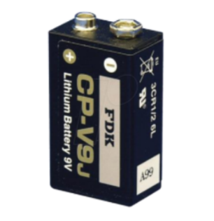](https://learn.digilabdte.com/uploads/images/gallery/2025-09/screenshot-2025-09-04-134946.png)
#### Cable
Cable (or jumper) is an electrical component that is used to connect between components, cable allows electrical current to flow from one component to another.
[](https://learn.digilabdte.com/uploads/images/gallery/2025-09/SsSimage.png)
#### Breadboard
Breadboard (or “Protoboard”) is a component that is used to attach electrical components such as jumper, transistor, resistor, IC etc. When using breadboards we don’t need to solder wires and components to make a circuit, because of this reason breadboards are widely used in prototyping a digital circuit.
[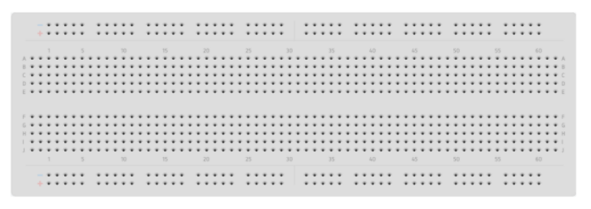](https://learn.digilabdte.com/uploads/images/gallery/2025-09/f2Kimage.png)
Breadboard consists of many holes and each hole is connected in a way to a metal plate. Not all holes in the breadboard are connected to each other, here is the picture of the breadboard's hole connections.
[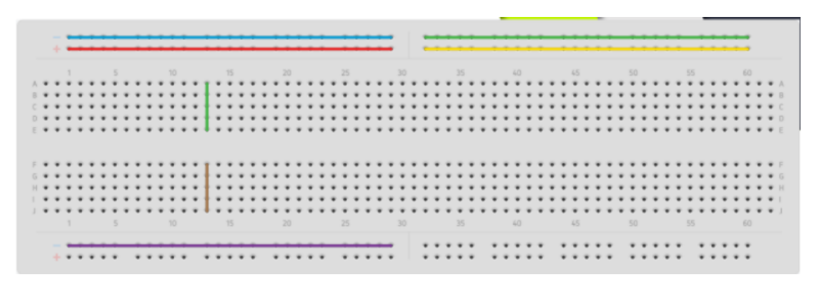](https://learn.digilabdte.com/uploads/images/gallery/2025-09/VURimage.png)
There are two kinds of connection in a breadboard, vertical and horizontal, the vertical connection is placed in the top and bottom part of the breadboard whereas the vertical connection is placed in the middle part.
If you look at the picture, holes that are connected to a line with the same color share the same connection, when one of the holes in that color is connected to an electric current the other holes from the same color lines will have the same amount of current.
#### Integrated Circuit
Integrated Circuit (IC) is an electrical component that consists of hundreds or even thousands of transistors, diodes, and resistors integrated to form a digital circuit that has its own function.
[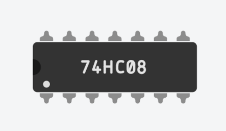](https://learn.digilabdte.com/uploads/images/gallery/2025-09/8Ysimage.png)
Every IC has many pins, and each pin has its own function. We can see the function of each pin from the datasheet provided by the manufacturer.
# 1.3 Datasheet
Datasheet is a piece of paper, in physical form or digital form, provided by the component or software manufacturer that consists of information about the product. In digital circuit design, datasheets provide information about electrical components such
as IC. How to read a datasheet:
#### Code
[](https://learn.digilabdte.com/uploads/images/gallery/2025-09/8fGimage.png)
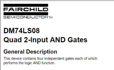
From the picture above we know that the IC code is 74LS08, in order to know the main function of the IC we only have to see the number from the code, for example the number from code 74LS08 is 7408, the 7408 IC code indicates that
the IC that described in the datasheet is a 2-Input AND Gates IC.
[](https://learn.digilabdte.com/uploads/images/gallery/2025-09/1Agimage.png)
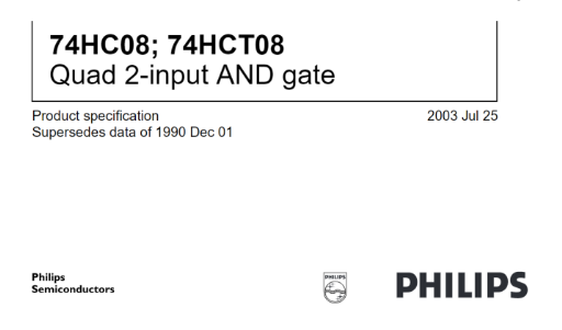
Another example is the 74HC08 IC, despite having a different code from the 75LS08 IC the main function is still the same, both used as a 2-Input AND Gates IC. Another example that you can search for yourself is the 74LS11 IC that acts as 3-input AND gates.
#### Main Function
[](https://learn.digilabdte.com/uploads/images/gallery/2025-09/NCnimage.png)
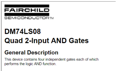
The main function of an IC can be identified from the title of the datasheet, 2-Input AND gates means that every gate in the IC consists only of two inputs while Quad means that there are 4 gates in that IC.
#### Truth Table
[](https://learn.digilabdte.com/uploads/images/gallery/2025-09/tzkimage.png)
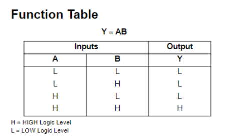
From the IC truth table we can identify the boolean function about the gates in that particular IC. for example the IC 7408 consist of 2-input AND gates and the output will be H (High) only when both the input is H (High) otherwise the output will be L (Low) when at least one of the input is L (Low), the truth table of an IC corresponds to the logic function of the gates.
#### Connection Diagram
[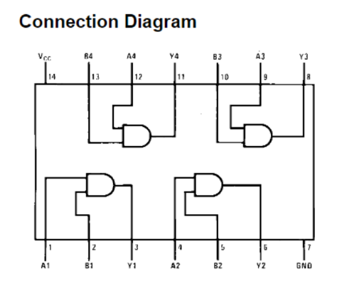](https://learn.digilabdte.com/uploads/images/gallery/2025-09/v9Timage.png)
Connection diagram berguna untuk mengetahui fungsi dari suatu pin, berdasarkan contoh, terlihat bahwa pin 14 dan pin 7 berfungsi sebagai vcc dan ground. The connection diagram is used to identify the function of a particular pin. From the picture above we can tell that pins 14 and 7 are used for VCC and ground, respectively.
# Module 2 - Boolean Algebra & Basic Logic Gates
# Objective
**1. Proof Boolean Algebra statements using basic logic gates.**
**2. Understand how to use Integrated Circuits (IC).**
# Theory
Boolean algebra is a mathematical system that describes the notations and operations on Boolean values. Boolean values are things that take on one out of two possible values. For example, a bit that can be a 1 or a 0.
Boolean algebra can be used to describe digital systems because digital signals are Boolean values: HIGH/VCC = 1 and LOW/GND = 0. So, a function of a digital system can be analyzed by using boolean algebra.
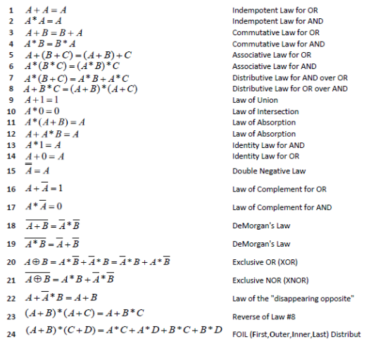
The laws of Boolean algebra are:
[](https://learn.digilabdte.com/uploads/images/gallery/2025-09/Ieuimage.png)
Those laws are used to simplify Boolean algebra expressions. The result is that the amount of components needed to implement a function into a digital system shrinks and so the cost for that system decreases. For example:
(A̅ + B) ∗ (A + B)
= B ∗ (A̅+ A) Inverse of Distributive Law for AND over OR
= B ∗ (1) Idempotent Law for OR
= B Identity Law for AND
Logic gates are the basic components that make up a digital system. A logic gate implements a logic operation. Below is a list of logic gates with its symbol, function, and truth table:
[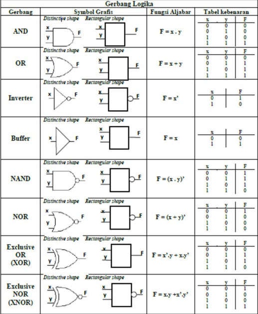](https://learn.digilabdte.com/uploads/images/gallery/2025-09/2uUimage.png)
# Module 3 - Karnaugh Map
By the end of this module, you will be able to:
1. Understand the purpose of a Karnaugh Map (K-Map) as a visual tool for simplifying digital logic.
2. Correctly create a K-Map for functions with 2, 3, or 4 input variables.
3. Translate a Boolean function or a truth table into its corresponding K-Map representation.
4. Apply the rules for grouping adjacent cells to find the simplest possible logic expression.
5. Use "don't care" conditions (X) effectively to achieve better simplification.
6. Derive the simplified Sum-of-Products (SOP) boolean function from a completed K-Map.
7. Recognize that a simplified function results in a more efficient electronic circuit with fewer logic gates.
# Objective
By the end of this module, you will be able to:
1. Understand the purpose of a Karnaugh Map (K-Map) as a visual tool for simplifying digital logic.
2. Correctly create a K-Map for functions with 2, 3, or 4 input variables.
3. Translate a Boolean function or a truth table into its corresponding K-Map representation.
4. Apply the rules for grouping adjacent cells to find the simplest possible logic expression.
5. Use "don't care" conditions (X) effectively to achieve better simplification.
6. Derive the simplified Sum-of-Products (SOP) boolean function from a completed K-Map.
7. Recognize that a simplified function results in a more efficient electronic circuit with fewer logic gates.
# What is a Karnaugh Map and Why Do We Use It?
In digital electronics, we often start with complex Boolean functions that describe how a circuit should behave. A complex function requires many logic gates (like AND, OR, NOT) to build. More gates mean the circuit is more expensive, consumes more power, and can be slower.
The Karnaugh Map (K-Map) is a graphical method used to simplify these complex Boolean functions. Think of it as a visual tool or a map that helps us see the simplest possible form of a function. By simplifying the function, we can build the same circuit with fewer gates, making it cheaper and more efficient. The K-Map is an easier and faster alternative to using Boolean algebra rules for simplification.
# The Structure of a K-Map
A K-Map is a table made of cells or boxes. Each cell represents one possible combination of inputs from a truth table.
The total number of cells is 2ⁿ, where n is the number of input variables.
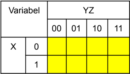
- For 2 variables (X, Y), we need 2² = 4 cells.
[](https://learn.digilabdte.com/uploads/images/gallery/2025-09/image-1758287483676.png)
.
- For 3 variables (X, Y, Z), we need 2³ = 8 cells.
[](https://learn.digilabdte.com/uploads/images/gallery/2025-09/image-1758287748148.png)
.
- For 4 variables (W, X, Y, Z), we need 2⁴ = 16 cells.
[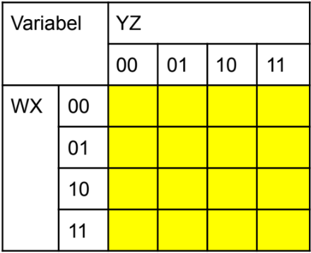](https://learn.digilabdte.com/uploads/images/gallery/2025-09/image-1758287799460.png)
A special rule for K-Maps is the way the rows and columns are labeled. The binary numbers are ordered so that only one bit changes between any two adjacent cells. This is why the labels are `00, 01, 11, 10` instead of the usual `00, 01, 10, 11`. This special ordering is the key that makes simplification possible.
This ordering also means the map "wraps around." The far-right column is considered adjacent to the far-left column, and the top row is adjacent to the bottom row.
# How to Simplify a Function Using a K-Map
We will focus on the `Sum-of-Products (SOP)` method, which involves looking for `1s` in the map.
**Step 1: Create and Fill the Map**\
Draw the correct K-Map for your number of variables. Look at your function's truth table or list of minterms. Place a `1` in every cell that corresponds to an output of `1`. If there are "don't care" conditions, place an `X` in those cells. Leave all other cells blank (or you can think of them as `0`s).\
[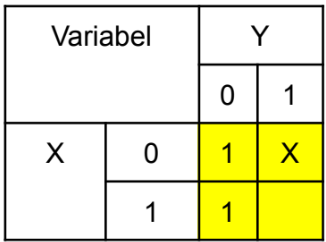](https://learn.digilabdte.com/uploads/images/gallery/2025-09/image-1758288416340.png)
**Step 2: Group the 1s**\
This is the most important step. You need to draw loops around groups of adjacent `1`s. Follow these rules:
- **Group Size:** Groups must contain a power-of-two number of cells (1, 2, 4, 8, or 16). You cannot have a group of 3, 5, or 6 cells.
- **Adjacency:** You can only group cells that are adjacent, either horizontally or vertically. Remember the "wrap-around" rule for the edges.
- **Make Groups as Large as Possible:** Always try to make the biggest groups you can. A single group of four is better than two separate groups of two.
- **Cover All 1s:** Every 1 on the map must be included in at least one group. A 1 can be part of multiple groups if it helps to make other groups larger.
- **Use Fewest Groups:** Your final goal is to cover all the 1s using the smallest number of groups possible.
- **Using "Don't Cares" (X):** You can include an X in a group if it helps you make a larger group of 1s. If an X doesn't help create a bigger group, just ignore it and treat it as a 0.\
[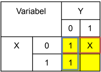](https://learn.digilabdte.com/uploads/images/gallery/2025-09/image-1758288467163.png)
**Step 3: Write the Simplified Function**\
Each group you created will become one term in your final simplified function. To find the term for each group:
1. Look at the variables along the rows and columns for that group.
2. Find the variable(s) that do not change their value inside the group.
3. If a variable stays as `1` for the entire group, include it as is (e.g., `A`).
4. If a variable stays as `0` for the entire group, include it with a NOT (e.g., `A'`).
5. If a variable changes its value (it is both `0` and `1`) within the group, it is eliminated from that term.
The final simplified function is the `OR (sum)` of all the terms you derived from each group.
# Module 4 - Complex Logic Gates
A complex logic gate is a digital circuit component that performs a logical function built from a combination of basic logic gates like AND, OR, and NOT. The most commonly used complex gates are NAND (Not-AND), NOR (Not-OR), XOR (Exclusive-OR), and XNOR (Exclusive-NOR).
The primary advantage of using complex gates is to simplify digital circuit design. By combining the functions of multiple basic gates into a single component, complex gates help reduce the total number of Integrated Circuits (ICs) needed to build a circuit. This makes the final circuit more compact, often more power-efficient, and potentially faster.
# Complex Logic ICs
### IC Functions, Pin Configurations, and Truth Tables
#### IC 7400: Quad 2-Input NAND Gate
**Function:** The IC 7400 contains four independent 2-input NAND gates in a single package. You can use any of these four gates separately.\
**Boolean Expression:** The logical function of a NAND gate is represented as `F = (AB)'`
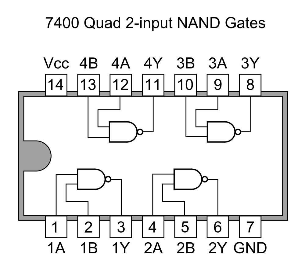
**Pin Configuration:** This IC has 14 pins.\
Pin 7: Ground connection (GND).\
Pin 14: Positive power supply (+5V, VCC).\
Gate 1: Pins 1 & 2 are inputs, Pin 3 is the output.\
Gate 2: Pins 4 & 5 are inputs, Pin 6 is the output.\
Gate 3: Pins 9 & 10 are inputs, Pin 8 is the output.\
Gate 4: Pins 12 & 13 are inputs, Pin 11 is the output.
**Truth Table:** The output is 0 only when both inputs are 1.
| Input A | Input B | Output Y |
|---------|---------|----------|
| 0 | 0 | 1 |
| 0 | 1 | 1 |
| 1 | 0 | 1 |
| 1 | 1 | 0 |
#### IC 7402: Quad 2-Input NOR Gate
**Function:** The IC 7402 contains four independent 2-input NOR gates.\
**Boolean Expression:** The logical function of a NOR gate is represented as `F = (A + B)'`
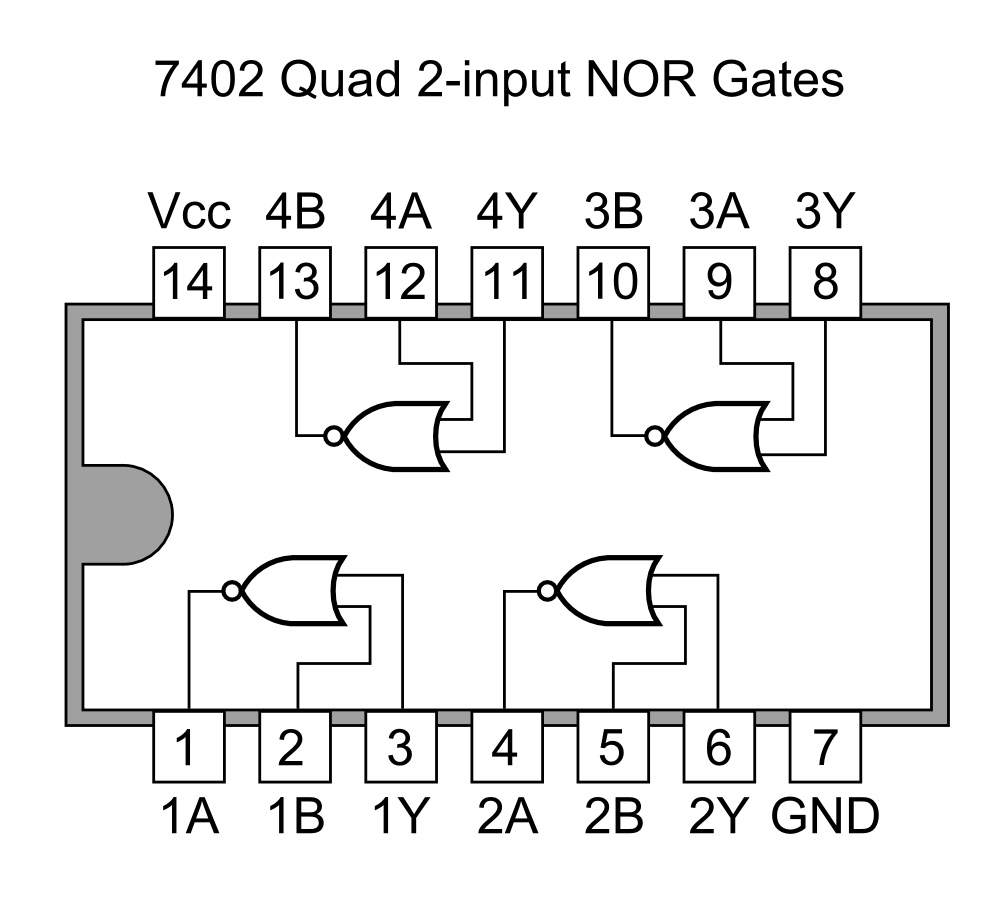
**Pin Configuration:** This 14-pin IC has a slightly **`different pinout`**.\
Pin 7: Ground connection (GND).\
Pin 14: Positive power supply (+5V, VCC).\
Gate 1: Pins 2 & 3 are inputs, Pin 1 is the output.\
Gate 2: Pins 5 & 6 are inputs, Pin 4 is the output.\
Gate 3: Pins 8 & 9 are inputs, Pin 10 is the output.\
Gate 4: Pins 11 & 12 are inputs, Pin 13 is the output.
**Truth Table:** The output is 1 only when both inputs are 0.
| Input A | Input B | Output Y |
|---------|---------|----------|
| 0 | 0 | 1 |
| 0 | 1 | 0 |
| 1 | 0 | 0 |
| 1 | 1 | 0 |
#### IC 7486: Quad 2-Input XOR Gate
**Function:** The IC 7486 contains four independent 2-input XOR (Exclusive-OR) gates.\
**Boolean Expression:** The logical function of a NAND gate is represented as `F = A'B + AB'`

**Pin Configuration:** The pinout for the 7486 is identical to the 7400.\
Pin 7: Ground connection (GND).\
Pin 14: Positive power supply (+5V, VCC).\
Gate 1: Pins 1 & 2 are inputs, Pin 3 is the output.\
Gate 2: Pins 4 & 5 are inputs, Pin 6 is the output.\
Gate 3: Pins 9 & 10 are inputs, Pin 8 is the output.\
Gate 4: Pins 12 & 13 are inputs, Pin 11 is the output.
**Truth Table:** The output is 1 only when the inputs are different.
| Input A | Input B | Output Y |
|---------|---------|----------|
| 0 | 0 | 0 |
| 0 | 1 | 1 |
| 1 | 0 | 1 |
| 1 | 1 | 0 |
#### IC 74266: Quad 2-Input XNOR Gate
**Function:** The IC 74266 contains four independent 2-input XNOR gates.\
**Boolean Expression:** The logical function of a NAND gate is represented as `F = AB + A'B'`

**Pin Configuration:** This 14-pin IC has a slightly **`different pinout`**.\
Pin 7: Ground connection (GND).\
Pin 14: Positive power supply (+5V, VCC).\
Gate 1: Pins 1 & 2 are inputs, Pin 3 is the output.\
Gate 2: Pins 5 & 6 are inputs, Pin 4 is the output.\
Gate 3: Pins 8 & 9 are inputs, Pin 10 is the output.\
Gate 4: Pins 12 & 13 are inputs, Pin 11 is the output.
**Truth Table:** The output is 1 only when the inputs are same.
| Input A | Input B | Output Y |
|---------|---------|----------|
| 0 | 0 | 1 |
| 0 | 1 | 0 |
| 1 | 0 | 0 |
| 1 | 1 | 1 |
# Complex vs Basic
### Advantages of Complex vs Basic Logic Gates
Using complex logic gates (like NAND, NOR, XOR) offers several significant advantages over building the same logic using only basic gates (AND, OR, NOT).
- **Reduced IC Count:** A single complex gate can perform the function of multiple basic gates. This means fewer physical chips are needed to build a circuit, which saves space on the circuit board.
- **Simplified Design:** Circuits built with fewer components are generally easier to design, read, and troubleshoot. The wiring is less complex, reducing the chances of errors.
- **Lower Cost:** Fewer ICs mean lower overall component cost for a project.
- **Increased Speed:** Every logic gate introduces a small time delay called "propagation delay." By reducing the total number of gates a signal must pass through, complex gates can often make the circuit operate faster.
- **Lower Power Consumption:** Since fewer ICs are used, the total power consumed by the circuit is typically lower.
# Complex is Universal
### Building Basic Gates from Universal Gates
NAND and NOR gates are called **universal gates** because any other logic function can be created using only one type of these gates.
#### Using Only NAND Gates
- **NOT Gate from NAND:** To create a NOT gate (an inverter), connect the two inputs of a single NAND gate together. This combined connection becomes the single input for your new NOT gate.
- **AND Gate from NAND:** To create an AND gate, use two NAND gates. First, connect your inputs (A and B) to the first NAND gate. The output of this gate is then connected to both inputs of a second NAND gate (which acts as a NOT gate). The final output is the AND function.
- **OR Gate from NAND:** To create an OR gate, use three NAND gates. First, create two separate NOT gates (one for input A, one for input B) by connecting the inputs of two NAND gates. Then, connect the outputs of these two inverters to the inputs of a third NAND gate.
#### Using Only NOR Gates
- **NOT Gate from NOR:** To create a NOT gate, connect the two inputs of a single NOR gate together.
- **OR Gate from NOR:** To create an OR gate, use two NOR gates. Connect your inputs (A and B) to the first NOR gate. Then, connect the output of that gate to both inputs of a second NOR gate (acting as a NOT gate).
- **AND Gate from NOR:** To create an AND gate, use three NOR gates. First, create two NOT gates (one for input A, one for input B). Connect the outputs of these inverters to the inputs of a third NOR gate.
| Gate | F = A + B | F = AB | F = A' |
|------|-----------|--------|--------|
| OR Gate | 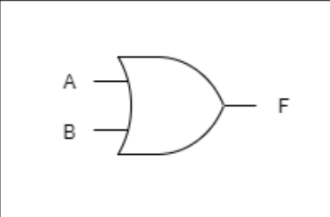 | - | - |
| AND Gate | - | 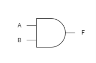 | - |
| NOT Gate | - | - | 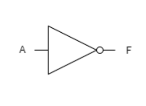 |
| NOR Gate | 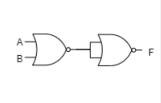 | 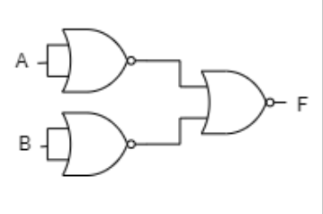 | 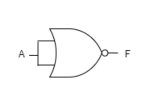 |
| NAND Gate | 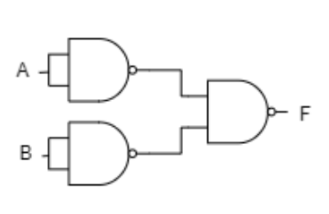 | 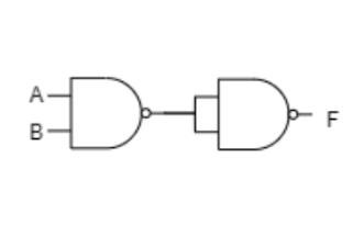 | 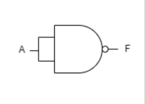 |
# Module 5 - Decoder & Encoder
# Module 6 - Multiplexer & Demultiplexer
Understand how Multiplexer and Demultiplexer works.
# Module 7 - Arithmetic Circuit
# Module 8 - Flip-Flop & Latch
# Module 9 - Register & Counter