Fundamentals of Digital Systems
- Module 1 : Introduction to Digital Circuit
- Module 2 : Boolean Algebra and Basic Logic Gates
- Module 3 : Karnaugh Map
- Module 4 : Complex Logic Gates
- Module 5 : Decoder & Encoder
- Module 6 : Multiplexer & Demultiplexer
- Module 7 : Digital Arithmetic Circuit
- Module 8 : Flip-Flop and Latch
- Module 9 : Register and Counter
Module 1 : Introduction to Digital Circuit
Learning Objectives :
1. Understand how to read a datasheet
2. Understand how an IC works
3. Understand how a breadboard works
Theory
Introduction to Digital Circuit : Theory
Introduction
Before we make a digital system circuit, we have to know more about the components that will be used to make them first.
1. Power Supply

Power supply is an electrical component that is used to supply electrical power for other components. The power supply that we mostly use in this lab are batteries and Arduino Uno. On a battery, there are two poles:
- Positive pole (VCC)
-
Negative pole (GND - Ground)
These poles will then be connected to the components accordingly.
2. Cable

Cable (or jumper cable) is an electrical component mostly used to connect other components. A cable allows electrical current to flow from one component to another. We'll use cables to connect each component until they become a singular circuit.
3. Breadboard
Breadboard (or "Protoboard") is a component used to attach electrical components such as jumpers, transistors, resistors, ICs, etc. into one place. When using breadboards, we don’t need to solder wires and components to make a circuit. Because of this reason, breadboards are widely used in prototyping digital circuits.

A breadboard consists of many holes, and each hole is connected in a specific way to a metal plate. Not all holes in the breadboard are connected to each other.

There are two kinds of connections in a breadboard: vertical and horizontal.
- The vertical connection is placed in the top and bottom parts of the breadboard.
- The horizontal connection is placed in the middle part.
If you look at the diagram, holes connected by the same colored line share the same connection. When one of the holes in that color is connected to an electric current, the other holes in the same color lines will receive the same amount of current.
4. Integrated Circuit (IC)

Integrated Circuits (IC) are various electrical components consisting of hundreds or even thousands of transistors, diodes, and resistors integrated to form a digital circuit with a specific function.
Every IC has multiple pins, each serving a distinct function. The function of each pin can be found in the datasheet provided by the manufacturer.
How to Read a Datasheet
1. Code

From the picture below, we know that the IC code is 74LS08. To determine the main function of the IC, we refer to the number in the code.
For example, in the 7408 IC, the number indicates that it is a 2-Input AND Gate IC.

Another example is the 74HC08 IC. Despite having a different prefix than 74LS08, both serve the same function as 2-Input AND Gate ICs.
A similar case is 74LS11, which functions as a 3-Input AND Gate IC.
2. Main Function
The main function of an IC can be identified from the title of the datasheet.

Example:
- "2-Input AND Gates" → Each gate in the IC consists of only two inputs.
- "Quad" → The IC contains four gates.
3. Truth Table
From the IC's truth table, we can determine the Boolean function of the gates in that IC.
For example, in the 7408 IC (2-Input AND Gate):
- The output is HIGH only when both inputs are HIGH.
- If at least one input is LOW, the output is LOW.
Truth Table Example:
| Input A | Input B | Output (AND) |
|---|---|---|
| L | L | L |
| L | H | L |
| H | L | L |
| H | H | H |
4. Connection Diagram
The connection diagram helps in identifying the function of each pin.

From the diagram, we see that:
- Pin 14 is used for VCC (power).
- Pin 7 is used for GND (ground).
How to Identify the Correct IC Pin Orientation
To correctly install an IC, we identify the correct pin orientation using:
- Notch

Ex: The pin on the top left is VCC, and bottom right is GND. Identifying which is the true orientation is crucial to determine the IC's pinout.
- Printed dot

- Printed text
While the printed text can help, it may fade over time. The most reliable way is by identifying the notch and dot positions.
Attachment
Datasheets:
- IC 74LS08: Datasheet Link
- IC 74HC08: Datasheet Link
- IC 74LS11: Datasheet Link
Online Tool:
- Tinkercad: Visit Tinkercad
Module 2 : Boolean Algebra and Basic Logic Gates
Learning Objectives :
1. Proving Boolean Algebra statements using basic logic gates.
2. Understand how to use Integrated Circuits (IC).
Video
Module 3 : Karnaugh Map
Video
Module 4 : Complex Logic Gates
Learning Objective:
1. Understand the principle of complex logic gates.
2. Understand NAND and NOR gates as universal gates.
Theory
Complex Logic Gates: Theory
Introduction
Complex logic gates are formed by combining basic logic gates like AND, OR, and NOT to create more advanced circuits that perform specific logical functions. These gates simplify digital circuit design and can reduce the number of integrated circuits (ICs) required.
Key Types of Complex Logic Gates
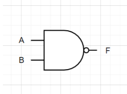
1. NAND Gate
A NAND gate is the combination of an AND gate followed by a NOT gate (inverter). It outputs a logic high (1) unless both inputs are high, making it a universal gate, as any logic gate can be constructed using only NAND gates.
| A | B | NAND |
|---|---|---|
| 0 | 0 | 1 |
| 0 | 1 | 1 |
| 1 | 0 | 1 |
| 1 | 1 | 0 |
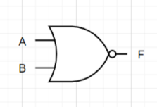
2. NOR Gate
A NOR gate is a combination of an OR gate followed by a NOT gate. It outputs a logic high (1) only when both inputs are low. Similar to the NAND gate, NOR can be used to construct any other basic gate.
| A | B | NOR |
|---|---|---|
| 0 | 0 | 1 |
| 0 | 1 | 0 |
| 1 | 0 | 0 |
| 1 | 1 | 0 |
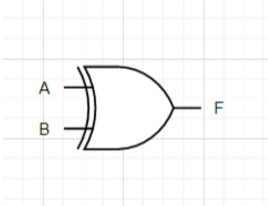
3. XOR Gate
An XOR (exclusive-OR) gate outputs true (1) when exactly one of the inputs is true. It's commonly used in arithmetic circuits and error detection.
| A | B | XOR |
|---|---|---|
| 0 | 0 | 0 |
| 0 | 1 | 1 |
| 1 | 0 | 1 |
| 1 | 1 | 0 |
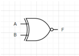
4. XNOR Gate
The XNOR (exclusive-NOR) gate is the complement of the XOR gate. It outputs true (1) only when the inputs are equal.
| A | B | XNOR |
|---|---|---|
| 0 | 0 | 1 |
| 0 | 1 | 0 |
| 1 | 0 | 0 |
| 1 | 1 | 1 |
Alternative Explanation of Logic Gates
Complex gates NAND and NOR can be used to represent basic logic gates functions AND, OR and NOT. The representation is shown below :
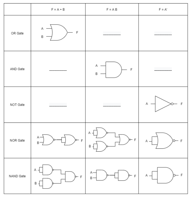
Importance of Complex Logic Gates
Complex gates, such as NAND and NOR, are known as universal gates because they can be used to implement any Boolean function or any other gate (AND, OR, NOT). They are particularly useful in optimizing the design of digital circuits by minimizing the number of components required.
In more advanced circuits, complex gates like XOR and XNOR play critical roles in error detection, data comparison, and arithmetic operations such as addition and subtraction which we will get into on the next module.
Conclusion
Complex logic gates offer an efficient way to design more intricate digital systems by reducing the complexity and number of ICs needed. Their versatility makes them essential building blocks in modern digital electronics.
Video
Module 5 : Decoder & Encoder
Learning Objectives :
1. Understand the working principles of decoders and encoders.
2. Being able to distinguish between a decoder and an encoder, as well as knowing when to use each one
Theory
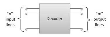
1. Decoder
In general, decoder is a combinatorial device that has n input ports and m output ports such that n <= m <= 2n. A decoder is commonly prefixed with the phrase n-to-m, where n and m are the number of input and output ports respectively.
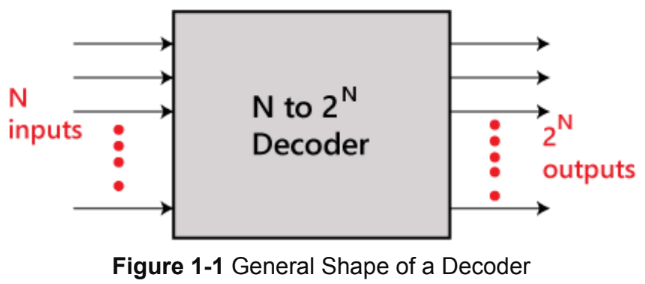
Decoders are used for decoding, which is a process of converting or “translating” an input code which is hard to deal with, to an output code which is easier to deal with. For example, a binary decoder is a type of decoder that converts an n-bit binary number to its corresponding minterm index or a one-hot representation of the number. So, a 3-to-8 binary decoder would have the truth table:
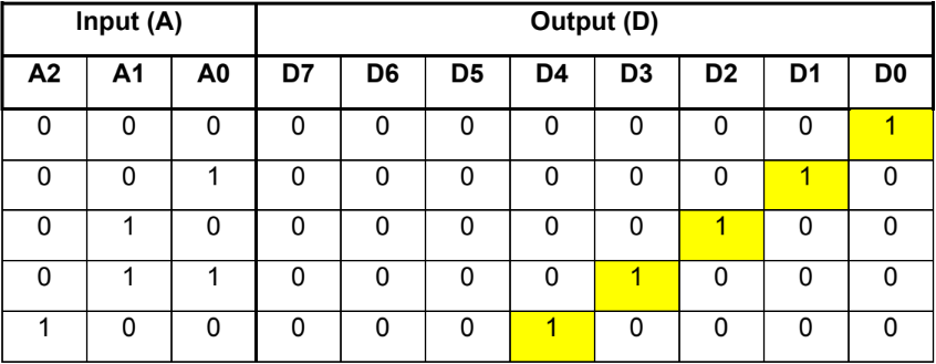
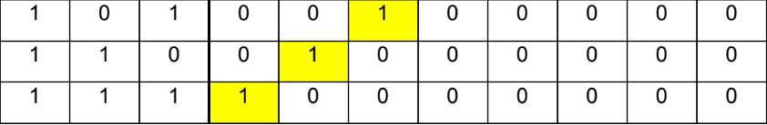
Explanation : If we’re looking for the number 5 (101), we just need to check port D5. If D5 is 0, then the number A is definitely not 5. If, however, D5 is 1, then it is certain that the number A is 5. Checking the output port D5 is easier than checking straight from the undecoded input. We would need to check if A2=1 AND A1=0 AND A0=1, which is tedious, especially for larger numbers with more bits.
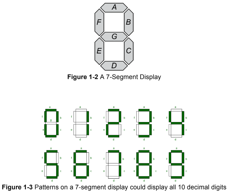
Another type of decoder is the 7-segment decoder. It converts a one-digit BCD (4-bit) input to a 7-bit output. Each output line correspond to a segment on a 7-segment display and when connected would result in a digit showing up in the display. For example, when the input is the number 5 (0101 in BCD), the output would light up appropriate segments of the display so that the actual “5” appears in it. Two such 7-segment decoders are IC 7447 and IC 7448
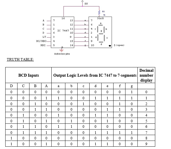
| Feature | IC 7447 | IC 7448 |
|---|---|---|
| Display Type | Common Anode | Common Cathode |
| Output Polarity | Active Low | Active High |
| Display Control | Turns on segments with logic 0 | Turns on segments with logic 1 |
| Usage | For displays with connected anodes | For displays with connected cathodes |
2. Encoder
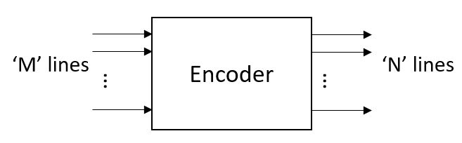
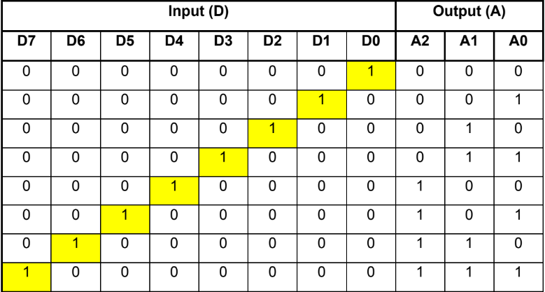
Encoder is the counterpart to the decoder; it does the inverse of what the decoder does, which is encoding. An encoder has m input lines and n output lines n <= m <= 2n. Like the decoder, encoder is usually prefixed with the phrase m-to-n, where m and n are the number of input and output ports respectively.
Generally, to encode means to take an input which has more lines/bits, to an output which has less lines/bits. This is done so that the resulting output could be transferred or transmitted to another location easily because it’s more packed and require less bits. For example, a binary encoder would output a binary number that correspond to the minterm index or one-hot representation of the input. So, an 8-to-3 binary encoder would have the truth table :
But, there’s a problem: not every input combination is defined in the truth table. For example, what would the output of the encoder be if 00000011 is given as the input? To solve that issue, we introduce a special type of encoder, called the priority encoder. It has the truth table :
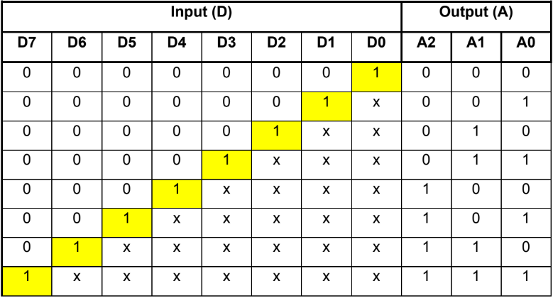
A priority encoder “prioritizes” input lines so that one line takes precedence over another. In this case, the input line with a bigger index takes precedence over the ones with a smaller index. If we take the example from before, when we give the priority encoder 00000011 as input, it “ignores” D0 and outputs 001. If we take another number: 10101010, then it would only “care” about D7 and ignore the rest. The resulting output would be 111.
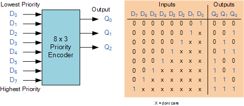
Priority encoders are available in standard IC form and the TTL 74LS148 is an 8-to-3 bit priority encoder which has eight active LOW (logic “0”) inputs and provides a 3-bit code of the highest ranked input at its output.
Additional Explanation
In addition to standard encoders like the priority encoder or decoders such as the BCD-to-7-segment decoder, we can create custom encoders and decoders based on specific application needs. These custom designs allow us to define unique encoding or decoding schemes that go beyond the limitations of previous standard examples & components (IC such as 7447,7448,74148) offering flexibility for various digital systems. Your Case Study or Additional Task and Final Project of this subject (Digital Systems Basics) will most likely need you to design these other than using the examples of decoder & encoder mentioned above.
Video
Module 6 : Multiplexer & Demultiplexer
Learning Objectives :
1. Understand how Multiplexer and Demultiplexer works.
2. Being able to distinguish between a Multiplexer and a Demultiplexer as well as knowing when to use each one.
Theory
1. Multiplexer
A multiplexer has multiple input pins, but only has one output pin. This circuit gives an output based on which input pin is chosen.
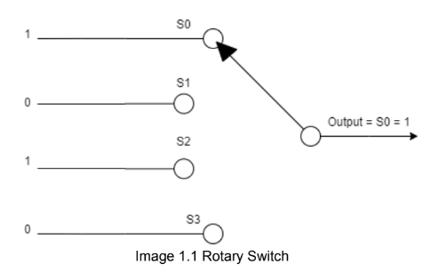
To explain further about how multiplexer works, we can imagine it as a rotary switch that works just like how multiplexers do. In the image above, there are 4 inputs from S0 to S3. Every input (from S0 to S3) has a signal between 1 or 0. The switch now is choosing to input S0, so the output of the rotary switch is the same as S0 (in this case is signal 1). Different from the rotary switch mentioned above, a multiplexer works by using a selector signal.
Multiplexers can also be built by primitive logic gates (AND, OR, NOT gates). To get the idea, see the image below (image 1.2).
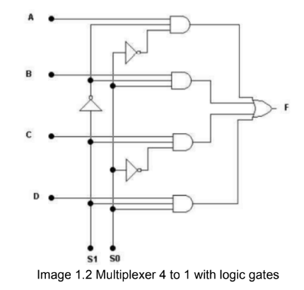
How a Multiplexer Works
- Input: The multiplexer receives multiple inputs, in this case/image above, its A to D.
- Selector: The selector signals determine which input will be passed to the output. In a 4-to-1 multiplexer, two selector signals (e.g., S1 and S0) are needed to select one of the four inputs.
- Output: Based on the combination of selector signals, the multiplexer forwards the value from the selected input to the output.
For example:
- If S1 = 0 and S0 = 0, input A is selected since its the first input (0 index, where 1st = 0, and 2nd = 1,etc).
- If S1 = 0 and S0 = 1, input B is selected since its the second input (0 index, where 1st = 0, and 2nd = 1,etc).
- And so on, with different selector combinations choosing different inputs.
Truth Table of a 4-to-1 Multiplexer
| S1 | S0 | Output |
|---|---|---|
| 0 | 0 | A |
| 0 | 1 | B |
| 1 | 0 | C |
| 1 | 1 | D |
Multiplexers are useful in digital applications, especially when managing multiple data sources that need to be routed to a single destination. Remember that to build a custom multiplexer with logic gates, we need to derive the boolean function first with a truth table.
2. Demultiplexer
A demultiplexer is the opposite of a multiplexer; it has one input pin and multiple output pins. The signal or data from the input pin is directed to the selected output pin. A selector signal is also used in a demultiplexer to determine which output pin will receive the input signal. The image below shows a logic gate diagram of a demultiplexer:

In this diagram, the signal on the IN pin will be transmitted to the chosen output. The output will be selected by the signals S0 and S1. In the circuit above, if an output pin is not selected, it will receive a signal of 0.
How a Demultiplexer Works
- Input: The demultiplexer takes a single input signal from the IN pin.
- Selector: The selector signals (S0 and S1) determine which output pin the input signal will be directed to.
- Outputs: The selected output pin receives the input signal, while the other output pins receive a signal of 0.
Truth Table of a 1-to-4 Demultiplexer
| S1 | S0 | Output 0 | Output 1 | Output 2 | Output 3 |
|---|---|---|---|---|---|
| 0 | 0 | IN | 0 | 0 | 0 |
| 0 | 1 | 0 | IN | 0 | 0 |
| 1 | 0 | 0 | 0 | IN | 0 |
| 1 | 1 | 0 | 0 | 0 | IN |
Thus, the demultiplexer enables the distribution of a single input signal to one of several output lines based on the selector signals.
Video
Module 7 : Digital Arithmetic Circuit
Learning Objective:
1. Understand basic digital arithmetic using adder and subtractor.
Theory
Objective
- Understand basic digital arithmetic using adders and subtractors.
In digital arithmetic, basic operations like addition, subtraction, multiplication, and division are all based on binary. These basic arithmetic operations are accomplished by using digital circuits called adders and subtractors.
1. Half Adder and Full Adder
In digital arithmetic, an adder is used to perform addition between 2 2-bit binary numbers. The half adder performs addition between bits A and B, producing outputs **S (sum) and C (carry). **
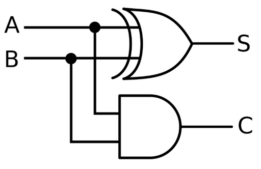
Figure 1-1: Half-Adder
Half-Adder Truth Table:
| A | B | S | C |
|---|---|---|---|
| 0 | 0 | 0 | 0 |
| 0 | 1 | 1 | 0 |
| 1 | 0 | 1 | 0 |
| 1 | 1 | 0 | 1 |
The simple adder adds the two bits together and represents them in sum (2^0) and carry (2^1).
Using this truth table, the half adder can be designed using Karnaugh maps, where the output S follows the logic of the XOR gate, and C follows the logic of the AND gate. In the half adder, we only consider inputs A and B.
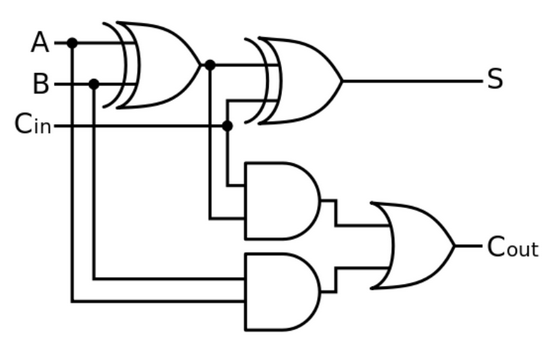
Figure 1-2: Full Adder
Truth Table for Full Adder:
| A | B | Cin | S | Cout |
|---|---|---|---|---|
| 0 | 0 | 0 | 0 | 0 |
| 0 | 0 | 1 | 1 | 0 |
| 0 | 1 | 0 | 1 | 0 |
| 0 | 1 | 1 | 0 | 1 |
| 1 | 0 | 0 | 1 | 0 |
| 1 | 0 | 1 | 0 | 1 |
| 1 | 1 | 0 | 0 | 1 |
| 1 | 1 | 1 | 1 | 1 |
The full adder is a more advanced version of the half-adder, having added carry-in and carry-out parts to accomodate higher level additions. By using full adders, a Ripple Carry Adder can be created by connecting Cout from the less significant bit to Cin of the more significant bit.
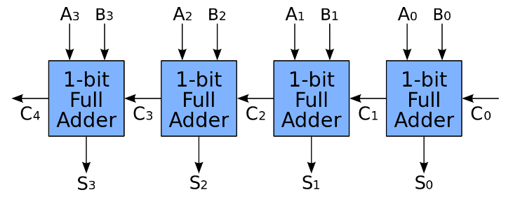
Figure 1-3: Ripple Carry Adder. We can analogize this as a chain of adders, each working on a different power of two (such as 2^3 <- 2^2 <- 2^1 <- 2^0).
2. Half and Full Subtractor
Opposite to adders, the subtractor is used to perform binary subtraction between 2 bits. A half subtractor performs subtraction between A and B, producing outputs D (difference) and Bo (borrow).
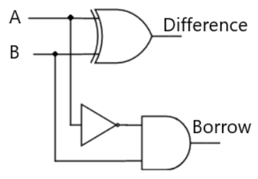
Figure 2-1: Half Subtractor
Truth Table for Half Subtractor:
| A | B | D | Bo |
|---|---|---|---|
| 0 | 0 | 0 | 0 |
| 0 | 1 | 1 | 1 |
| 1 | 0 | 1 | 0 |
| 1 | 1 | 0 | 0 |
Here, through boolean simplification / K-Map, D follows the same logic as the XOR gate, and Bo follows the logic A' . B.
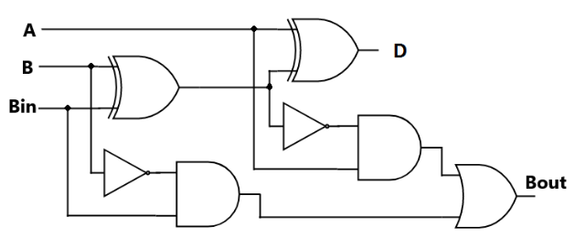
Figure 2-2: Full Subtractor
Truth Table for Full Subtractor:
| A | B | Bin | D | Bout |
|---|---|---|---|---|
| 0 | 0 | 0 | 0 | 0 |
| 0 | 0 | 1 | 1 | 1 |
| 0 | 1 | 0 | 1 | 1 |
| 0 | 1 | 1 | 0 | 1 |
| 1 | 0 | 0 | 1 | 0 |
| 1 | 0 | 1 | 0 | 0 |
| 1 | 1 | 0 | 0 | 0 |
| 1 | 1 | 1 | 1 | 1 |
Like the full adder, the full subtractor has an additional input, Bin (borrow in), which comes from the Bout of another full subtractor. By using full subtractors, a Ripple Borrow Subtractor can be created by connecting Bout from the less significant bit to Bin of the more significant bit.
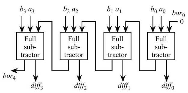
Figure 2-3: Ripple Borrow Subtractor
Video
Module 8 : Flip-Flop and Latch
Learning Objectives:
1. Understand the working principles of sequential circuits.
2. Understand the differences between sequential circuits and combinatorial
circuits.
3. Understand how latches and flip-flops work as the base component that
compose sequential circuits and memory devices.
Theory
A. Introduction to Sequential Circuits
If we have an AND gate and drive both inputs with 1, the output would be 1. However, if one of its inputs is 0, the output will be 0. This behavior is defined by the truth table and describes a combinatorial circuit, where the output is determined solely by its inputs.
Sequential circuits are different. They not only rely on the current inputs but also the previous output. For example, creating a circuit that flips every time a button is pressed, changing from 0 to 1 or 1 to 0, requires remembering the previous output. This type of circuit, where the output is determined by both inputs and the previous output, is called a sequential circuit.
B. The Clock Signal
The clock signal is a periodic signal used to synchronize digital circuits, analogous to a musical tempo in an orchestra. It pulses at precise intervals to ensure sequential circuits remain in sync.
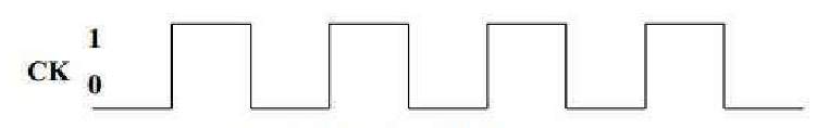
Figure 1-1: Clock Diagram
The clock signal is a square wave, with a rising edge (transition from 0 to 1) and a falling edge (transition from 1 to 0).
One prominent example is the CPU clock, which pulses in MHz to GHz, controlling instruction execution in processors.
C. Synchronous and Asynchronous Sequential Circuits
Sequential circuits can be either synchronous or asynchronous. Synchronous circuits are controlled by a clock signal, while asynchronous circuits are not.
There are two types of synchronous circuits:
- Positive edge triggered: Activated on the rising edge of the clock signal.
- Negative edge triggered: Activated on the falling edge of the clock signal.
Synchronous circuits have a triangle symbol at the clock input, and a bubble at the clock input of negative edge-triggered devices.
Below is the picture for the two types of synchronous sequential circuits. The left one is positive edge triggered and the right one is negative edge triggered. Notice the “bubble” at the clock input of the negative edge triggered device.
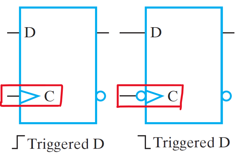 Figure 2-1: Trigger Types
D. Latches and Flip-Flops
Latches and flip-flops are the simplest sequential circuits. They store a single bit of data (either 0 or 1) and are essential components in building more complex sequential circuits and memory devices (akin to logic gates, but for sequential circuits). The key difference between them is that latches are asynchronous, while flip-flops are synchronous.
Latches and flip-flops have a characteristic equation that relates the next state (NS/Qnext) to the present state (PS/Q).
1. SR Latch and SR' Latch
An SR latch is built from two cross-coupled NOR gates. It has two inputs, S (set) and R (reset), and two outputs, Q and Q', which are complements of each other.
- When
S = 1andR = 0,Q = 1(set state). - When
S = 0andR = 1,Q = 0(reset state). - When
S = 0andR = 0, the latch retains its previous state.
If both S = 1 and R = 1, the state is undefined (forbidden).
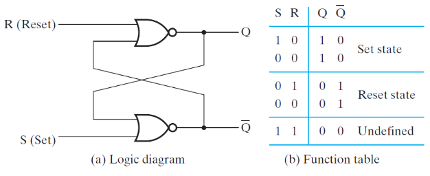
Figure 3-1: SR Latch
The characteristic equation for the SR latch is:
Q_next = S + R'Q, where S.R = 0.
A similar type, the (SR)' latch is built from cross-coupled NAND gates. It is activated when inputs are driven low (0), unlike the SR latch.
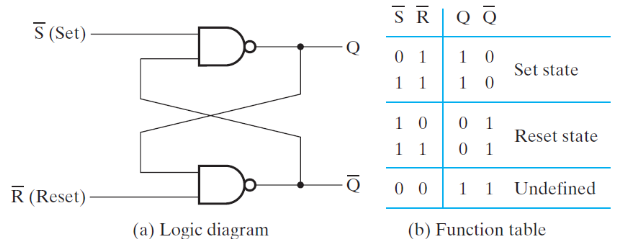
Figure 3-2: (SR') Latch
2. D Latch
A D latch avoids the undefined state by ensuring S and R are never both 1 at the same time. The D latch is created by using an inverter to make S and R complements of each other.
It has two inputs:
- D (data): Determines the next state.
- C (control): Enables or disables state changes.
When C = 0, the latch holds its state. When C = 1, the output depends on D:
-
D = 0results in a reset state (Q = 0). -
D = 1results in a set state (Q = 1).
The characteristic equation for the D latch is:
Q_next = D.
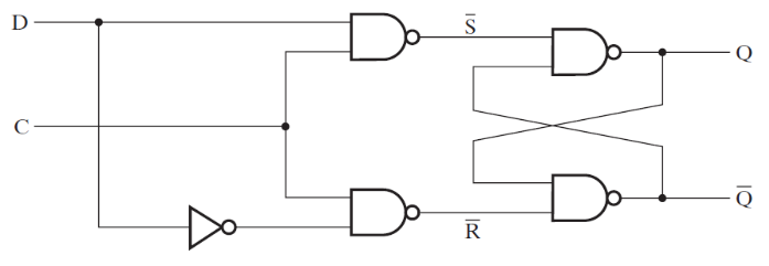
Figure 3-3-1: D Latch
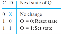
Figure 3-3-2: D Latch Truth Table
3. D Flip-Flop
A D flip-flop operates like a D latch but with a clock signal instead of an enable signal. The state changes at the transition of the clock signal (rising or falling edge), depending on D.
The D flip-flop can be implemented by using two latches (in this case a D latch and an SR latch) in a configuration as shown below:
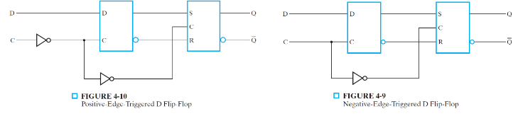
Figure 3-4: D Flip-Flop
It prevents multiple state changes during a clock cycle by using two latches (a D latch and an SR latch) in a master-slave configuration.
4. JK Flip-Flop
The JK flip-flop is similar to the SR flip-flop, but when both J and K are 1, it enters a toggle state where the output flips between 0 and 1 on each clock cycle.
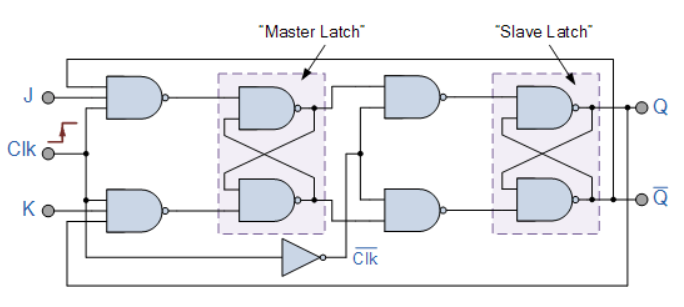
Figure 3-5-1: JK Flip-Flop
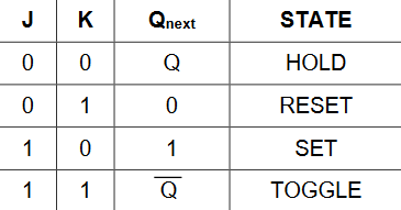
Figure 3-5-2: JK Truth Table
The characteristic equation for the JK flip-flop is:
Q_next = JQ' + K'Q.
5. T Flip-Flop
The T flip-flop has two states:
-
Hold (
T = 0): Retains the previous state. -
Toggle (
T = 1): Inverts the previous state.
The T flip-flop can be created by connecting a JK flip-flop’s J and K inputs together or using an XOR gate with a D flip-flop.
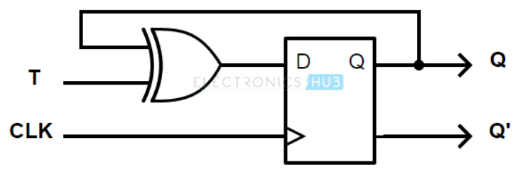
Figure 3-6-1: T Flip-Flop
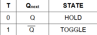
Figure 3-6-2: T Flip-Flop Truth Table
The characteristic equation for the T flip-flop is:
Q_next = T ⊕ Q.
Module 9 : Register and Counter
Learning Objectives:
- Understand the concept of parallel and serial binary operations
- Understand a combination and conversion of parallel and binary operations
Theory
A. Binary Operation
In electrical components, data is represented as a stream of bits. These bits are processed in the components, creating processed bits of data. This process is called a binary operation. Binary operations are further classified into:
1. Parallel Operation
The parallel operation works instantly without a timer. Input bits are processed together at the same time, producing output bits in a short amount of time. This operation is very effective for quick outputs but is expensive for larger bits.
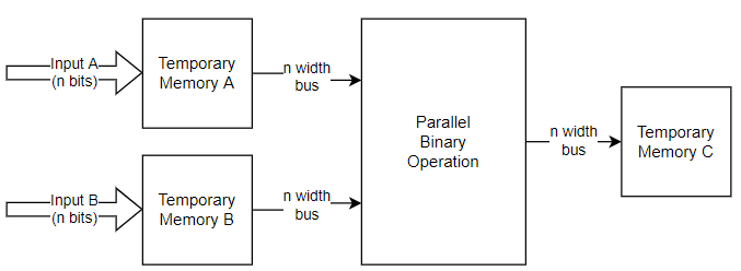
Figure 1-1: Parallel Operation Block Diagram In this design type, optimized design is key to produce efficient and cost effective designs.
2. Serial Operation
In serial operation, input bits are processed one by one, creating output sequentially. A timer ensures that the input produces the correct output and shifts the data in the correct order. Memory is also needed to store the input and output bits, often achieved using a shift register.
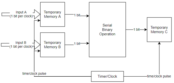 Figure 1-2: Serial Operation Block Diagram
The block doesn’t need a timer pulse since it works instantly for every input change. The output is also saved at every pulse, sequentially.
Figure 1-2: Serial Operation Block Diagram
The block doesn’t need a timer pulse since it works instantly for every input change. The output is also saved at every pulse, sequentially.
3. Combination
A combination of parallel and serial operations can be used to balance speed and cost. This hybrid operation requires a timer to mark the beginning and end of the serial part before and after the parallel part.
B. Register
To save data in a digital circuit, a register is used. A register saves data using signal bits with flip-flops and states. Registers can be designed using a combination of serial and parallel operations, such as Serial Input Parallel Output (SIPO) and Parallel Input Serial Output (PISO) registers.
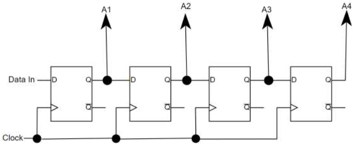
Figure 2-1: SIPO Register
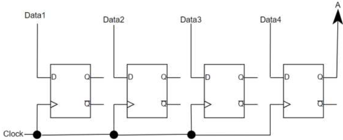
Figure 2-2: PISO Register
The main component of a register is the flip flop, a clock (or enabler), input, and output. The main difference between parallel and serial is how the signal is handled. If more than one signal is handled simultaneously, then it is called parallel. If only one signal is handled one by one, then it is called serial.
C. Counter
A counter is used to control sequences and execution steps in a logical circuit by counting bits. Counters consist of flip-flops that switch states in sequence. There are two types of counters:
- Synchronous Counter: All flip-flops are connected and controlled at the same time by the same external clock.
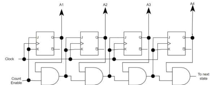
Figure 3-1: 4-bit Synchronous Counter
- Asynchronous Counter: Flip-flops are controlled by the output of the previous flip-flop, except for the first one, which is controlled by an external clock.
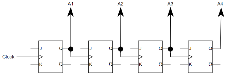
Figure 3-2: 4-bit Asynchronous Counter
Counters can count up, count down, or both, and may use different coding schemes, such as n-bit binary counters or n-bit BCD counters. A counter that counts from 0 to 9 (0000 to 1001) is called a decade counter.
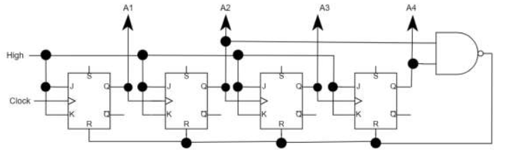
Figure 4-1: 4-bit Decade Counter