Theory
A. Introduction to Sequential Circuits
If we have an AND gate and drive both inputs with 1, the output would be 1. However, if one of its inputs is 0, the output will be 0. This behavior is defined by the truth table and describes a combinatorial circuit, where the output is determined solely by its inputs.
Sequential circuits are different. They not only rely on the current inputs but also the previous output. For example, creating a circuit that flips every time a button is pressed, changing from 0 to 1 or 1 to 0, requires remembering the previous output. This type of circuit, where the output is determined by both inputs and the previous output, is called a sequential circuit.
B. The Clock Signal
The clock signal is a periodic signal used to synchronize digital circuits, analogous to a musical tempo in an orchestra. It pulses at precise intervals to ensure sequential circuits remain in sync.

Figure 1-1: Clock Diagram
The clock signal is a square wave, with a rising edge (transition from 0 to 1) and a falling edge (transition from 1 to 0).
One prominent example is the CPU clock, which pulses in MHz to GHz, controlling instruction execution in processors.
C. Synchronous and Asynchronous Sequential Circuits
Sequential circuits can be either synchronous or asynchronous. Synchronous circuits are controlled by a clock signal, while asynchronous circuits are not.
There are two types of synchronous circuits:
- Positive edge triggered: Activated on the rising edge of the clock signal.
- Negative edge triggered: Activated on the falling edge of the clock signal.
Synchronous circuits have a triangle symbol at the clock input, and a bubble at the clock input of negative edge-triggered devices.
Below is the picture for the two types of synchronous sequential circuits. The left one is positive edge triggered and the right one is negative edge triggered. Notice the “bubble” at the clock input of the negative edge triggered device.
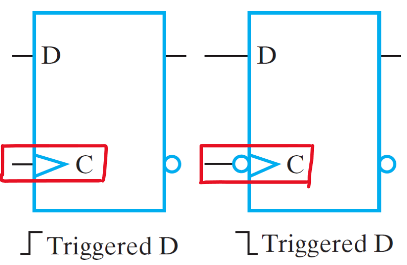 Figure 2-1: Trigger Types
D. Latches and Flip-Flops
Latches and flip-flops are the simplest sequential circuits. They store a single bit of data (either 0 or 1) and are essential components in building more complex sequential circuits and memory devices (akin to logic gates, but for sequential circuits). The key difference between them is that latches are asynchronous, while flip-flops are synchronous.
Latches and flip-flops have a characteristic equation that relates the next state (NS/Qnext) to the present state (PS/Q).
1. SR Latch and SR' Latch
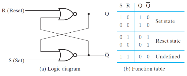
An SR latch is built from two cross-coupled NOR gates. It has two inputs, S (set) and R (reset), and two outputs, Q and Q', which are complements of each other.
- When
S = 1andR = 0,Q = 1(set state). - When
S = 0andR = 1,Q = 0(reset state). - When
S = 0andR = 0, the latch retains its previous state.
If both S = 1 and R = 1, the state is undefined (forbidden).
Figure 3-1: SR Latch
The characteristic equation for the SR latch is:
Q_next = S + R'Q, where S.R = 0.
A similar type, the (SR)' latch is built from cross-coupled NAND gates. It is activated when inputs are driven low (0), unlike the SR latch.
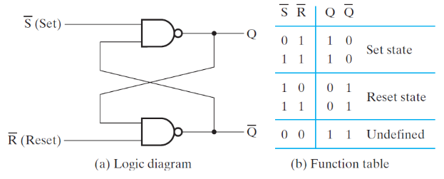
Figure 3-2: (SR') Latch
2. D Latch
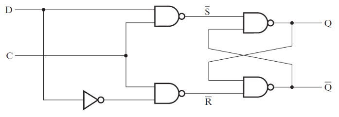
A D latch avoids the undefined state by ensuring S and R are never both 1 at the same time. The D latch is created by using an inverter to make S and R complements of each other.
It has two inputs:
- D (data): Determines the next state.
- C (control): Enables or disables state changes.
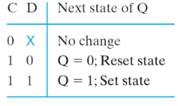
When C = 0, the latch holds its state. When C = 1, the output depends on D:
-
D = 0results in a reset state (Q = 0). -
D = 1results in a set state (Q = 1).
The characteristic equation for the D latch is:
Q_next = D.
Figure 3-3-1: D Latch
Figure 3-3-2: D Latch Truth Table
3. D Flip-Flop
A D flip-flop operates like a D latch but with a clock signal instead of an enable signal. The state changes at the transition of the clock signal (rising or falling edge), depending on D.
The D flip-flop can be implemented by using two latches (in this case a D latch and an SR latch) in a configuration as shown below:

Figure 3-4: D Flip-Flop
It prevents multiple state changes during a clock cycle by using two latches (a D latch and an SR latch) in a master-slave configuration.
4. JK Flip-Flop
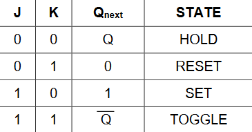
The JK flip-flop is similar to the SR flip-flop, but when both J and K are 1, it enters a toggle state where the output flips between 0 and 1 on each clock cycle.
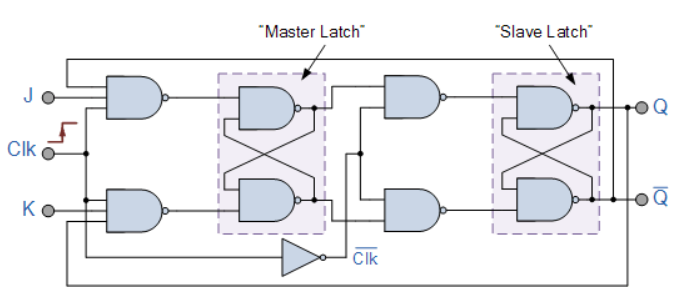
Figure 3-5-1: JK Flip-Flop
Figure 3-5-2: JK Truth Table
The characteristic equation for the JK flip-flop is:
Q_next = JQ' + K'Q.
5. T Flip-Flop
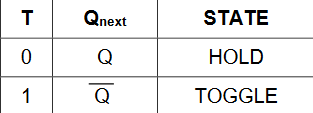
The T flip-flop has two states:
-
Hold (
T = 0): Retains the previous state. -
Toggle (
T = 1): Inverts the previous state.
The T flip-flop can be created by connecting a JK flip-flop’s J and K inputs together or using an XOR gate with a D flip-flop.
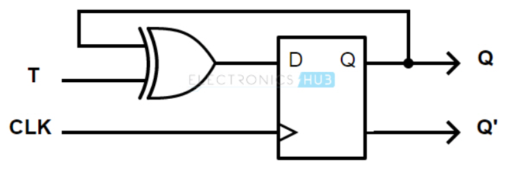
Figure 3-6-1: T Flip-Flop
Figure 3-6-2: T Flip-Flop Truth Table
The characteristic equation for the T flip-flop is:
Q_next = T ⊕ Q.

